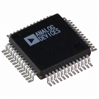
ADUC836BSZ Analog Devices Inc, ADUC836BSZ Datasheet - Page 20

ADUC836BSZ
Manufacturer Part Number
ADUC836BSZ
Description
16bit Dual ADC With Embedded 8 Bit MCU
Manufacturer
Analog Devices Inc
Series
MicroConverter® ADuC8xxr
Datasheet
1.ADUC836BSZ.pdf
(80 pages)
Specifications of ADUC836BSZ
Core Processor
8052
Core Size
8-Bit
Speed
12.58MHz
Connectivity
EBI/EMI, I²C, SPI, UART/USART
Peripherals
POR, PSM, PWM, Temp Sensor, WDT
Number Of I /o
34
Program Memory Size
62KB (62K x 8)
Program Memory Type
FLASH
Eeprom Size
4K x 8
Ram Size
2.25K x 8
Voltage - Supply (vcc/vdd)
2.7 V ~ 5.25 V
Data Converters
A/D 7x16b; D/A 1x12b
Oscillator Type
Internal
Operating Temperature
-40°C ~ 125°C
Package / Case
52-MQFP, 52-PQFP
Cpu Family
ADuC8xx
Device Core
8052
Device Core Size
8b
Frequency (max)
12.58MHz
Interface Type
I2C/SPI/UART
Total Internal Ram Size
2.25KB
# I/os (max)
26
Number Of Timers - General Purpose
3
Operating Supply Voltage (typ)
3.3/5V
Operating Supply Voltage (max)
5.25V
Operating Supply Voltage (min)
2.7V
On-chip Adc
2(2-chx16-bit)
On-chip Dac
1-chx12-bit
Instruction Set Architecture
CISC
Operating Temp Range
-40C to 125C
Operating Temperature Classification
Automotive
Mounting
Surface Mount
Pin Count
52
Package Type
MQFP
Package
52MQFP
Family Name
ADuC8xx
Maximum Speed
12.58 MHz
Operating Supply Voltage
3.3|5 V
Data Bus Width
8 Bit
Number Of Programmable I/os
26
Number Of Timers
3
Lead Free Status / RoHS Status
Lead free / RoHS Compliant
Lead Free Status / RoHS Status
Lead free / RoHS Compliant
Available stocks
Company
Part Number
Manufacturer
Quantity
Price
Company:
Part Number:
ADUC836BSZ
Manufacturer:
ADI
Quantity:
150
Company:
Part Number:
ADUC836BSZ
Manufacturer:
Analog Devices Inc
Quantity:
10 000
Part Number:
ADUC836BSZ
Manufacturer:
ADI/亚德诺
Quantity:
20 000
ADC0H/ADC0M (Primary ADC Conversion Result Registers)
These two 8-bit registers hold the 16-bit conversion result from the primary ADC.
SFR Address
Power-On Default Value
Bit Addressable
ADC1H/ADC1L (Auxiliary ADC Conversion Result Registers)
These two 8-bit registers hold the 16-bit conversion result from the auxiliary ADC.
SFR Address
Power-On Default Value
Bit Addressable
OF0H/OF0M (Primary ADC Offset Calibration Registers*)
These two 8-bit registers hold the 16-bit offset calibration coefficient for the primary ADC. These registers are configured at power-on
with a factory default value of 800000H. However, these bytes will be automatically overwritten if an internal or system zero-scale
calibration of the primary ADC is initiated by the user via MD2–0 bits in the ADCMODE Register.
SFR Address
Power-On Default Value
Bit Addressable
OF1H/OF1L (Auxiliary ADC Offset Calibration Registers*)
These two 8-bit registers hold the 16-bit offset calibration coefficient for the auxiliary ADC. These registers are configured at power-on
with a factory default value of 8000H. However, these bytes will be automatically overwritten if an internal or system zero-scale calibration
of the auxiliary ADC is initiated by the user via the MD2–0 bits in the ADCMODE Register.
SFR Address
Power-On Default Value
Bit Addressable
GN0H/GN0M (Primary ADC Gain Calibration Registers*)
These two 8-bit registers hold the 16-bit gain calibration coefficient for the primary ADC. These registers are configured at power-on
with a factory-calculated internal full-scale calibration coefficient. Every device will have an individual coefficient. However, these bytes
will be automatically overwritten if an internal or system full-scale calibration of the primary ADC is initiated by the user via MD2–0
bits in the ADCMODE Register.
SFR Address
Power-On Default Value
Bit Addressable
GN1H/GN1L (Auxiliary ADC Gain Calibration Registers*)
These two 8-bit registers hold the 16-bit gain calibration coefficient for the auxiliary ADC. These registers are configured at power-on
with a factory-calculated internal full-scale calibration coefficient. Every device will have an individual coefficient. However, these bytes
will be automatically overwritten if an internal or system full-scale calibration of the auxiliary ADC is initiated by the user via MD2–0
bits in the ADCMODE Register.
SFR Address
Power-On Default Value
Bit Addressable
*These registers can be overwritten by user software only if Mode bits MD0–2 (ADCMODE SFR) are zero.
ADuC836
ADC0M
ADC1L
ADC0H
00H
No
ADC1H
00H
No
OF0H
OF0M
80000H
No
OF1H
OF1L
8000H
No
GN0H
GN0M
No
GN1H
GN1L
No
High Data Byte
Middle Data Byte
ADC0H, ADC0M
ADC0H, ADC0M
High Data Byte
Low Data Byte
ADC1H, ADC1L
ADC1H, ADC1L
Primary ADC Offset Coefficient High Byte
Primary ADC Offset Coefficient Middle Byte
OF0H, OF0M respectively
OF0H, OF0M
Auxiliary ADC Offset Coefficient High Byte
Auxiliary ADC Offset Coefficient Low Byte
OF1H and OF1L, respectively
OF1H, OF1L
Primary ADC Gain Coefficient High Byte
Primary ADC Gain Coefficient Middle Byte
Configured at Factory Final Test; See Notes above.
GN0H, GN0M
Auxiliary ADC Gain Coefficient High Byte
Auxiliary ADC Gain Coefficient Low Byte
Configured at Factory Final Test; see notes above.
GN1H, GN1L
–20–
DBH
DAH
DDH
DCH
E3H
E2H
E5H
E4H
EBH
EAH
EDH
ECH
REV. A


