ATMEGA168PA-PU Atmel, ATMEGA168PA-PU Datasheet - Page 311
ATMEGA168PA-PU
Manufacturer Part Number
ATMEGA168PA-PU
Description
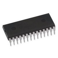
MCU, 8BIT, AVR, 16K FLASH, 28PDIP
Manufacturer
Atmel
Datasheet
1.ATMEGA48A-PU.pdf
(566 pages)
Specifications of ATMEGA168PA-PU
Controller Family/series
Atmega
No. Of I/o's
23
Eeprom Memory Size
512Byte
Ram Memory Size
1KB
Cpu Speed
20MHz
No.
RoHS Compliant
Core Size
8bit
Program Memory Size
16KB
Oscillator Type
External, Internal
Rohs Compliant
Yes
Available stocks
Company
Part Number
Manufacturer
Quantity
Price
Company:

Part Number:
ATMEGA168PA-PU
Manufacturer:
TI
Quantity:
1 240


27.7.15
27.8
8271C–AVR–08/10
Serial Downloading
Parallel Programming Characteristics
For characteristics of the Parallel Programming, see
page
Both the Flash and EEPROM memory arrays can be programmed using the serial SPI bus while
RESET is pulled to GND. The serial interface consists of pins SCK, MOSI (input) and MISO (out-
put). After RESET is set low, the Programming Enable instruction needs to be executed first
before program/erase operations can be executed. NOTE, in
mapping for SPI programming is listed. Not all parts use the SPI pins dedicated for the internal
SPI interface.
Figure 27-7. Serial Programming and Verify
Notes:
When programming the EEPROM, an auto-erase cycle is built into the self-timed programming
operation (in the Serial mode ONLY) and there is no need to first execute the Chip Erase
instruction. The Chip Erase operation turns the content of every memory location in both the
Program and EEPROM arrays into 0xFF.
Depending on CKSEL Fuses, a valid clock must be present. The minimum low and high periods
for the serial clock (SCK) input are defined as follows:
Low: > 2 CPU clock cycles for f
High: > 2 CPU clock cycles for f
ATmega48A/48PA/88A/88PA/168A/168PA/328/328
329.
1. If the device is clocked by the internal Oscillator, it is no need to connect a clock source to the
2. V
XTAL1 pin.
CC
- 0.3V <
AV
CC
< V
MOSI
MISO
SCK
ck
ck
CC
< 12 MHz, 3 CPU clock cycles for f
< 12 MHz, 3 CPU clock cycles for f
+ 0.3V, however,
XTAL1
RESET
GND
(1)
AV
CC
”Parallel Programming Characteristics” on
AVCC
VCC
should always be within 1.8 - 5.5V
+1.8 - 5.5V
+1.8 - 5.5V
Table 27-17 on page
(2)
ck
ck
>= 12 MHz
>= 12 MHz
312, the pin
311
Related parts for ATMEGA168PA-PU
Image
Part Number
Description
Manufacturer
Datasheet
Request
R

Part Number:
Description:
Manufacturer:
Atmel Corporation
Datasheet:
Part Number:
Description:
Manufacturer:
Atmel Corporation
Datasheet:
Part Number:
Description:
Manufacturer:
ATMEL Corporation
Datasheet:

Part Number:
Description:
IC AVR MCU 16K 20MHZ 32TQFP
Manufacturer:
Atmel
Datasheet:

Part Number:
Description:
IC AVR MCU 16K 20MHZ 32-QFN
Manufacturer:
Atmel
Datasheet:

Part Number:
Description:
IC AVR MCU 16K 20MHZ 28DIP
Manufacturer:
Atmel
Datasheet:
Part Number:
Description:
MCU AVR 16K FLASH 15MHZ 32-TQFP
Manufacturer:
Atmel
Datasheet:

Part Number:
Description:
MCU AVR 16K FLASH 15MHZ 32-QFN
Manufacturer:
Atmel
Datasheet:
Part Number:
Description:
IC AVR MCU 16K 20MHZ 32TQFP
Manufacturer:
Atmel
Datasheet:

Part Number:
Description:
MCU AVR 16KB FLASH 20MHZ 32QFN
Manufacturer:
Atmel
Datasheet:
Part Number:
Description:
MCU AVR 16KB FLASH 20MHZ 32TQFP
Manufacturer:
Atmel
Datasheet:

Part Number:
Description:
IC MCU AVR 16K FLASH 32-QFN
Manufacturer:
Atmel
Datasheet: