ATMEGA168PA-PU Atmel, ATMEGA168PA-PU Datasheet - Page 254
ATMEGA168PA-PU
Manufacturer Part Number
ATMEGA168PA-PU
Description
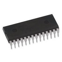
MCU, 8BIT, AVR, 16K FLASH, 28PDIP
Manufacturer
Atmel
Datasheet
1.ATMEGA48A-PU.pdf
(566 pages)
Specifications of ATMEGA168PA-PU
Controller Family/series
Atmega
No. Of I/o's
23
Eeprom Memory Size
512Byte
Ram Memory Size
1KB
Cpu Speed
20MHz
No.
RoHS Compliant
Core Size
8bit
Program Memory Size
16KB
Oscillator Type
External, Internal
Rohs Compliant
Yes
Available stocks
Company
Part Number
Manufacturer
Quantity
Price
Company:

Part Number:
ATMEGA168PA-PU
Manufacturer:
TI
Quantity:
1 240


23.4
8271C–AVR–08/10
Prescaling and Conversion Timing
If Auto Triggering is enabled, single conversions can be started by writing ADSC in ADCSRA to
one. ADSC can also be used to determine if a conversion is in progress. The ADSC bit will be
read as one during a conversion, independently of how the conversion was started.
Figure 23-3. ADC Prescaler
By default, the successive approximation circuitry requires an input clock frequency between 50
kHz and 200 kHz to get maximum resolution. If a lower resolution than 10 bits is needed, the
input clock frequency to the ADC can be higher than 200 kHz to get a higher sample rate.
The ADC module contains a prescaler, which generates an acceptable ADC clock frequency
from any CPU frequency above 100 kHz. The prescaling is set by the ADPS bits in ADCSRA.
The prescaler starts counting from the moment the ADC is switched on by setting the ADEN bit
in ADCSRA. The prescaler keeps running for as long as the ADEN bit is set, and is continuously
reset when ADEN is low.
When initiating a single ended conversion by setting the ADSC bit in ADCSRA, the conversion
starts at the following rising edge of the ADC clock cycle.
A normal conversion takes 13 ADC clock cycles. The first conversion after the ADC is switched
on (ADEN in ADCSRA is set) takes 25 ADC clock cycles in order to initialize the analog circuitry.
When the bandgap reference voltage is used as input to the ADC, it will take a certain time for
the voltage to stabilize. If not stabilized, the first value read after the first conversion may be
wrong.
The actual sample-and-hold takes place 1.5 ADC clock cycles after the start of a normal conver-
sion and 13.5 ADC clock cycles after the start of an first conversion. When a conversion is
complete, the result is written to the ADC Data Registers, and ADIF is set. In Single Conversion
mode, ADSC is cleared simultaneously. The software may then set ADSC again, and a new
conversion will be initiated on the first rising ADC clock edge.
When Auto Triggering is used, the prescaler is reset when the trigger event occurs. This assures
a fixed delay from the trigger event to the start of conversion. In this mode, the sample-and-hold
takes place two ADC clock cycles after the rising edge on the trigger source signal. Three addi-
tional CPU clock cycles are used for synchronization logic.
ATmega48A/48PA/88A/88PA/168A/168PA/328/328
ADEN
START
ADPS0
ADPS1
ADPS2
CK
Reset
7-BIT ADC PRESCALER
ADC CLOCK SOURCE
254
Related parts for ATMEGA168PA-PU
Image
Part Number
Description
Manufacturer
Datasheet
Request
R

Part Number:
Description:
Manufacturer:
Atmel Corporation
Datasheet:
Part Number:
Description:
Manufacturer:
Atmel Corporation
Datasheet:
Part Number:
Description:
Manufacturer:
ATMEL Corporation
Datasheet:

Part Number:
Description:
IC AVR MCU 16K 20MHZ 32TQFP
Manufacturer:
Atmel
Datasheet:

Part Number:
Description:
IC AVR MCU 16K 20MHZ 32-QFN
Manufacturer:
Atmel
Datasheet:

Part Number:
Description:
IC AVR MCU 16K 20MHZ 28DIP
Manufacturer:
Atmel
Datasheet:
Part Number:
Description:
MCU AVR 16K FLASH 15MHZ 32-TQFP
Manufacturer:
Atmel
Datasheet:

Part Number:
Description:
MCU AVR 16K FLASH 15MHZ 32-QFN
Manufacturer:
Atmel
Datasheet:
Part Number:
Description:
IC AVR MCU 16K 20MHZ 32TQFP
Manufacturer:
Atmel
Datasheet:

Part Number:
Description:
MCU AVR 16KB FLASH 20MHZ 32QFN
Manufacturer:
Atmel
Datasheet:
Part Number:
Description:
MCU AVR 16KB FLASH 20MHZ 32TQFP
Manufacturer:
Atmel
Datasheet:

Part Number:
Description:
IC MCU AVR 16K FLASH 32-QFN
Manufacturer:
Atmel
Datasheet: