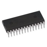
ATMEGA168PA-PU Atmel, ATMEGA168PA-PU Datasheet - Page 16

ATMEGA168PA-PU
Manufacturer Part Number
ATMEGA168PA-PU
Description
MCU, 8BIT, AVR, 16K FLASH, 28PDIP
Manufacturer
Atmel
Datasheet
1.ATMEGA48A-PU.pdf
(566 pages)
Specifications of ATMEGA168PA-PU
Controller Family/series
Atmega
No. Of I/o's
23
Eeprom Memory Size
512Byte
Ram Memory Size
1KB
Cpu Speed
20MHz
No.
RoHS Compliant
Core Size
8bit
Program Memory Size
16KB
Oscillator Type
External, Internal
Rohs Compliant
Yes
Available stocks
Company
Part Number
Manufacturer
Quantity
Price
Company:
Part Number:
ATMEGA168PA-PU
Manufacturer:
TI
Quantity:
1 240
- Current page: 16 of 566
- Download datasheet (23Mb)
7. AVR Memories
7.1
7.2
8271C–AVR–08/10
Overview
In-System Reprogrammable Flash Program Memory
T h i s
ATmega48A/48PA/88A/88PA/168A/168PA/328/328P. The AVR architecture has two main
memory spaces, the Data Memory and the Program Memory space. In addition, the
ATmega48A/48PA/88A/88PA/168A/168PA/328/328P features an EEPROM Memory for data
storage. All three memory spaces are linear and regular.
The ATmega48A/48PA/88A/88PA/168A/168PA/328/328P contains 4/8/16/32K bytes On-chip
In-System Reprogrammable Flash memory for program storage. Since all AVR instructions are
16 or 32 bits wide, the Flash is organized as 2/4/8/16K x 16. For software security, the Flash
Program memory space is divided into two sections, Boot Loader Section and Application Pro-
gram Section in ATmega88PA and ATmega168PA. See SELFPRGEN description in section
”SPMCSR – Store Program Memory Control and Status Register” on page 294
The Flash memory has an endurance of at least 10,000 write/erase cycles. The
ATmega48A/48PA/88A/88PA/168A/168PA/328/328P Program Counter (PC) is 11/12/13/14 bits
wide, thus addressing the 2/4/8/16K program memory locations. The operation of Boot Program
section and associated Boot Lock bits for software protection are described in detail in
gramming the Flash, ATmega 48A/48PA” on page 270
Write Self-Programming” on page
description on Flash Programming in SPI- or Parallel Programming mode.
Constant tables can be allocated within the entire program memory address space (see the LPM
– Load Program Memory instruction description).
Timing diagrams for instruction fetch and execution are presented in
ing” on page
ATmega48A/48PA/88A/88PA/168A/168PA/328/328
s e c t i o n
13.
d e s c r i b e s
279.
”Memory Programming” on page 296
t h e
d i f f e r e n t
and
”Boot Loader Support – Read-While-
m e m o r i e s
”Instruction Execution Tim-
contains a detailed
for more details.
i n
”Self-Pro-
t h e
16
Related parts for ATMEGA168PA-PU
Image
Part Number
Description
Manufacturer
Datasheet
Request
R

Part Number:
Description:
Manufacturer:
Atmel Corporation
Datasheet:

Part Number:
Description:
Manufacturer:
Atmel Corporation
Datasheet:

Part Number:
Description:
Manufacturer:
ATMEL Corporation
Datasheet:

Part Number:
Description:
IC AVR MCU 16K 20MHZ 32TQFP
Manufacturer:
Atmel
Datasheet:

Part Number:
Description:
IC AVR MCU 16K 20MHZ 32-QFN
Manufacturer:
Atmel
Datasheet:

Part Number:
Description:
IC AVR MCU 16K 20MHZ 28DIP
Manufacturer:
Atmel
Datasheet:

Part Number:
Description:
MCU AVR 16K FLASH 15MHZ 32-TQFP
Manufacturer:
Atmel
Datasheet:

Part Number:
Description:
MCU AVR 16K FLASH 15MHZ 32-QFN
Manufacturer:
Atmel
Datasheet:

Part Number:
Description:
IC AVR MCU 16K 20MHZ 32TQFP
Manufacturer:
Atmel
Datasheet:

Part Number:
Description:
MCU AVR 16KB FLASH 20MHZ 32QFN
Manufacturer:
Atmel
Datasheet:

Part Number:
Description:
MCU AVR 16KB FLASH 20MHZ 32TQFP
Manufacturer:
Atmel
Datasheet:

Part Number:
Description:
IC MCU AVR 16K FLASH 32-QFN
Manufacturer:
Atmel
Datasheet:


