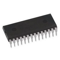
ATMEGA168PA-PU Atmel, ATMEGA168PA-PU Datasheet - Page 277

ATMEGA168PA-PU
Manufacturer Part Number
ATMEGA168PA-PU
Description
MCU, 8BIT, AVR, 16K FLASH, 28PDIP
Manufacturer
Atmel
Datasheet
1.ATMEGA48A-PU.pdf
(566 pages)
Specifications of ATMEGA168PA-PU
Controller Family/series
Atmega
No. Of I/o's
23
Eeprom Memory Size
512Byte
Ram Memory Size
1KB
Cpu Speed
20MHz
No.
RoHS Compliant
Core Size
8bit
Program Memory Size
16KB
Oscillator Type
External, Internal
Rohs Compliant
Yes
Available stocks
Company
Part Number
Manufacturer
Quantity
Price
Company:
Part Number:
ATMEGA168PA-PU
Manufacturer:
TI
Quantity:
1 240
- Current page: 277 of 566
- Download datasheet (23Mb)
25.3
25.3.1
8271C–AVR–08/10
Register Description
SPMCSR – Store Program Memory Control and Status Register
The Store Program Memory Control and Status Register contains the control bits needed to con-
trol the Program memory operations.
• Bit 7 – SPMIE: SPM Interrupt Enable
When the SPMIE bit is written to one, and the I-bit in the Status Register is set (one), the SPM
ready interrupt will be enabled. The SPM ready Interrupt will be executed as long as the SELF-
PRGEN bit in the SPMCSR Register is cleared. The interrupt will not be generated during
EEPROM write or SPM.
• Bit 6 – RWWSB: Read-While-Write Section Busy
This bit is for compatibility with devices supporting Read-While-Write. It will always read as zero
in ATmega 48A/48PA.
• Bit 5 – Reserved
This bit is a reserved bit in the ATmega48A/48PA/88A/88PA/168A/168PA/328/328P and will
always read as zero.
• Bit 4 – RWWSRE: Read-While-Write Section Read Enable
The functionality of this bit in ATmega 48A/48PA is a subset of the functionality in
ATmega88A/88PA/168A/168PA/328/328P. If the RWWSRE bit is written while filling the tempo-
rary page buffer, the temporary page buffer will be cleared and the data will be lost.
• Bit 3 – BLBSET: Boot Lock Bit Set
The functionality of this bit in ATmega 48A/48PA is a subset of the functionality in
ATmega88A/88PA/168A/168PA/328/328P. An LPM instruction within three cycles after BLBSET
and SELFPRGEN are set in the SPMCSR Register, will read either the Lock bits or the Fuse bits
(depending on Z0 in the Z-pointer) into the destination register. See
Bits from Software” on page 272
• Bit 2 – PGWRT: Page Write
If this bit is written to one at the same time as SELFPRGEN, the next SPM instruction within four
clock cycles executes Page Write, with the data stored in the temporary buffer. The page
address is taken from the high part of the Z-pointer. The data in R1 and R0 are ignored. The
PGWRT bit will auto-clear upon completion of a Page Write, or if no SPM instruction is executed
within four clock cycles. The CPU is halted during the entire Page Write operation.
• Bit 1 – PGERS: Page Erase
If this bit is written to one at the same time as SELFPRGEN, the next SPM instruction within four
clock cycles executes Page Erase. The page address is taken from the high part of the Z-
pointer. The data in R1 and R0 are ignored. The PGERS bit will auto-clear upon completion of a
ATmega48A/48PA/88A/88PA/168A/168PA/328/328
Bit
0x37 (0x57)
Read/Write
Initial Value
SPMIE
R/W
7
0
RWWSB
R
6
0
for details.
R
5
–
0
RWWSRE
R/W
4
0
BLBSET
R/W
3
0
PGWRT
R/W
2
0
”Reading the Fuse and Lock
PGERS
R/W
1
0
SELFPRGEN
R/W
0
0
SPMCSR
277
Related parts for ATMEGA168PA-PU
Image
Part Number
Description
Manufacturer
Datasheet
Request
R

Part Number:
Description:
Manufacturer:
Atmel Corporation
Datasheet:

Part Number:
Description:
Manufacturer:
Atmel Corporation
Datasheet:

Part Number:
Description:
Manufacturer:
ATMEL Corporation
Datasheet:

Part Number:
Description:
IC AVR MCU 16K 20MHZ 32TQFP
Manufacturer:
Atmel
Datasheet:

Part Number:
Description:
IC AVR MCU 16K 20MHZ 32-QFN
Manufacturer:
Atmel
Datasheet:

Part Number:
Description:
IC AVR MCU 16K 20MHZ 28DIP
Manufacturer:
Atmel
Datasheet:

Part Number:
Description:
MCU AVR 16K FLASH 15MHZ 32-TQFP
Manufacturer:
Atmel
Datasheet:

Part Number:
Description:
MCU AVR 16K FLASH 15MHZ 32-QFN
Manufacturer:
Atmel
Datasheet:

Part Number:
Description:
IC AVR MCU 16K 20MHZ 32TQFP
Manufacturer:
Atmel
Datasheet:

Part Number:
Description:
MCU AVR 16KB FLASH 20MHZ 32QFN
Manufacturer:
Atmel
Datasheet:

Part Number:
Description:
MCU AVR 16KB FLASH 20MHZ 32TQFP
Manufacturer:
Atmel
Datasheet:

Part Number:
Description:
IC MCU AVR 16K FLASH 32-QFN
Manufacturer:
Atmel
Datasheet:


