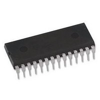
ATMEGA168PA-PU Atmel, ATMEGA168PA-PU Datasheet - Page 19

ATMEGA168PA-PU
Manufacturer Part Number
ATMEGA168PA-PU
Description
MCU, 8BIT, AVR, 16K FLASH, 28PDIP
Manufacturer
Atmel
Datasheet
1.ATMEGA48A-PU.pdf
(566 pages)
Specifications of ATMEGA168PA-PU
Controller Family/series
Atmega
No. Of I/o's
23
Eeprom Memory Size
512Byte
Ram Memory Size
1KB
Cpu Speed
20MHz
No.
RoHS Compliant
Core Size
8bit
Program Memory Size
16KB
Oscillator Type
External, Internal
Rohs Compliant
Yes
Available stocks
Company
Part Number
Manufacturer
Quantity
Price
Company:
Part Number:
ATMEGA168PA-PU
Manufacturer:
TI
Quantity:
1 240
- Current page: 19 of 566
- Download datasheet (23Mb)
7.3.1
7.4
7.4.1
8271C–AVR–08/10
EEPROM Data Memory
Data Memory Access Times
EEPROM Read/Write Access
This section describes the general access timing concepts for internal memory access. The
internal data SRAM access is performed in two clk
Figure 7-4.
The ATmega48A/48PA/88A/88PA/168A/168PA/328/328P contains 256/512/512/1K bytes of
data EEPROM memory. It is organized as a separate data space, in which single bytes can be
read and written. The EEPROM has an endurance of at least 100,000 write/erase cycles. The
access between the EEPROM and the CPU is described in the following, specifying the
EEPROM Address Registers, the EEPROM Data Register, and the EEPROM Control Register.
”Memory Programming” on page 296
in SPI or Parallel Programming mode.
The EEPROM Access Registers are accessible in the I/O space.
The write access time for the EEPROM is given in
lets the user software detect when the next byte can be written. If the user code contains instruc-
tions that write the EEPROM, some precautions must be taken. In heavily filtered power
supplies, V
period of time to run at a voltage lower than specified as minimum for the clock frequency used.
See
situations.
In order to prevent unintentional EEPROM writes, a specific write procedure must be followed.
Refer to the description of the EEPROM Control Register for details on this.
When the EEPROM is read, the CPU is halted for four clock cycles before the next instruction is
executed. When the EEPROM is written, the CPU is halted for two clock cycles before the next
instruction is executed.
ATmega48A/48PA/88A/88PA/168A/168PA/328/328
”Preventing EEPROM Corruption” on page 20
CC
Address
clk
is likely to rise or fall slowly on power-up/down. This causes the device for some
On-chip Data SRAM Access Cycles
Data
Data
WR
CPU
RD
Compute Address
T1
Memory Access Instruction
contains a detailed description on EEPROM Programming
Address valid
CPU
for details on how to avoid problems in these
T2
Table
cycles as described in
7-2. A self-timing function, however,
Next Instruction
T3
Figure
7-4.
19
Related parts for ATMEGA168PA-PU
Image
Part Number
Description
Manufacturer
Datasheet
Request
R

Part Number:
Description:
Manufacturer:
Atmel Corporation
Datasheet:

Part Number:
Description:
Manufacturer:
Atmel Corporation
Datasheet:

Part Number:
Description:
Manufacturer:
ATMEL Corporation
Datasheet:

Part Number:
Description:
IC AVR MCU 16K 20MHZ 32TQFP
Manufacturer:
Atmel
Datasheet:

Part Number:
Description:
IC AVR MCU 16K 20MHZ 32-QFN
Manufacturer:
Atmel
Datasheet:

Part Number:
Description:
IC AVR MCU 16K 20MHZ 28DIP
Manufacturer:
Atmel
Datasheet:

Part Number:
Description:
MCU AVR 16K FLASH 15MHZ 32-TQFP
Manufacturer:
Atmel
Datasheet:

Part Number:
Description:
MCU AVR 16K FLASH 15MHZ 32-QFN
Manufacturer:
Atmel
Datasheet:

Part Number:
Description:
IC AVR MCU 16K 20MHZ 32TQFP
Manufacturer:
Atmel
Datasheet:

Part Number:
Description:
MCU AVR 16KB FLASH 20MHZ 32QFN
Manufacturer:
Atmel
Datasheet:

Part Number:
Description:
MCU AVR 16KB FLASH 20MHZ 32TQFP
Manufacturer:
Atmel
Datasheet:

Part Number:
Description:
IC MCU AVR 16K FLASH 32-QFN
Manufacturer:
Atmel
Datasheet:


