TMOV25SP385M Littelfuse Inc, TMOV25SP385M Datasheet - Page 14
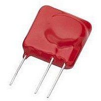
TMOV25SP385M
Manufacturer Part Number
TMOV25SP385M
Description
TMOV VARISTOR PB FREE 25S
Manufacturer
Littelfuse Inc
Series
iTMOV®r
Specifications of TMOV25SP385M
Varistor Voltage
682V
Current-surge
20kA
Number Of Circuits
1
Maximum Ac Volts
385VAC
Energy
430J
Package / Case
Disc 25mm 3-Lead
Suppressor Type
Varistor
Peak Surge Current @ 8/20µs
20000A
Varistor Case
25mm DISC
Clamping Voltage Vc Max
1010V
Peak Energy (10/1000us)
430J
Voltage Rating Vdc
682V
Voltage Rating Vac
385V
Lead Free Status / RoHS Status
Lead free / RoHS Compliant
Maximum Dc Volts
-
Lead Free Status / Rohs Status
Lead free / RoHS Compliant


Introduction to Varistor Technology
I
The symmetrical, sharp breakdown characteristics shown
in Figure 1, enable the varistor to provide excellent tran-
sient suppression performance. When exposed to high
voltage transients the varistor impedance changes many
orders of magnitude from a near open circuit to a highly
conductive level, thus clamping the transient voltage to a
safe level. The potentially destructive energy of the incom-
ing transient pulse is absorbed by the varistor, thereby
protecting vulnerable circuit components.
Since electrical conduction occurs, in effect, between
Z
the Littelfuse Varistor is inherently more rugged than its
single P–N junction counterparts, such as Zener diodes.
In the varistor, energy is absorbed uniformly throughout
the body of the device with the resultant heating spread
evenly through its volume. Electrical properties are con-
trolled mainly by the physical dimensions of the varistor
body which is sintered in various form factors such as
discs, chips and tubes. The energy rating is determined by
volume, voltage rating by thickness or current flow path
length, and current capability by area measured normal to
the direction of current flow.
The varistor body structure consists of a matrix of con-
ductive Z
ing P–N junction semiconductor characteristics. These
boundaries are responsible for blocking conduction at low
voltages and are the source of the nonlinear electrical
conduction at higher voltages.
N
FIGURE 1. TYPICAL VARISTOR V-I CHARACTERISTIC
O grains distributed throughout the bulk of the device,
N
O grains separated by grain boundaries provid-
V
PER VERT
DIV 1mA
PER HORIZ
DIV 50V
PER STEP
gm PER DIV
Revision: November 5, 2009
Varistor Products
10
Physical Properties
MOVs are designed to protect sensitive circuits against
external transients (lightning) and internal transients
(inductive load switching, relay switching and capaci-
tor discharges). And other high level transients found in
industrial, AC line application or lower level transients found
in automotive DC line applications with peak current rating
ranging from 20A to 500A and peak energy rating from
0.05J – 2.5J.
An attractive property of the MOV is that the electrical char-
acteristics are related to the bulk of the device. Each ZnO
grain of the ceramic acts as if it has a semiconductor junc-
tion at the grain boundary. A cross-section of the material
is shown in Figure 2, which illustrates the ceramic micro-
structure. Varistors are fabricated by forming and sintering
Zinc Oxide-based powders into ceramic parts. These parts
are then electroded with either thick film Silver or arc/flame
sprayed metal.
The ZnO grain boundaries can be clearly observed. Since
the nonlinear electrical behavior occurs at the boundary
of each semiconducting ZnO grain, the varistor can be
considered a "multi-junction" device composed of many
series and parallel connections of grain boundaries. Device
behavior may be analyzed with respect to the details of
the ceramic microstructure. Mean grain size and grain size
distribution play a major role in electrical behavior.
FIGURE 2. OPTICAL PHOTOMICROGRAPH OF A POLISHED
AND ETCHED SECTION OF A VARISTOR
Please refer to www.littelfuse.com for current information.
Specifications are subject to change without notice.
100μ
©2009 Littelfuse, Inc.
Related parts for TMOV25SP385M
Image
Part Number
Description
Manufacturer
Datasheet
Request
R

Part Number:
Description:
FUSEHOLDER 20A MINI INLINE CRIMP
Manufacturer:
Littelfuse Inc
Datasheet:

Part Number:
Description:
FUSEHOLDER BODY ATO INLINE PNLMT
Manufacturer:
Littelfuse Inc
Datasheet:

Part Number:
Description:
FUSE 2A 63V FAST 1206
Manufacturer:
Littelfuse Inc
Datasheet:
Part Number:
Description:
FUSE 1.25A 63V FAST 1206
Manufacturer:
Littelfuse Inc
Datasheet:
Part Number:
Description:
FUSE .250A 125V FAST 1206
Manufacturer:
Littelfuse Inc
Datasheet:
Part Number:
Description:
FUSE 4A 32V FAST 1206
Manufacturer:
Littelfuse Inc
Datasheet:
Part Number:
Description:
FUSE 1.75A 63V FAST 1206
Manufacturer:
Littelfuse Inc
Datasheet:

Part Number:
Description:
FUSE 1A 32V FST 0603 LEADFREE TR
Manufacturer:
Littelfuse Inc
Datasheet:

Part Number:
Description:
FUSE 1A 32V FAST SLIM 0402
Manufacturer:
Littelfuse Inc
Datasheet:

Part Number:
Description:
FUSE 2A 125V FAST NANO2 SMD
Manufacturer:
Littelfuse Inc
Datasheet:

Part Number:
Description:
FUSE .250A 125V FAST NANO2 SMD
Manufacturer:
Littelfuse Inc
Datasheet:

Part Number:
Description:
FUSE .500A 125V FAST NANO2 SMD
Manufacturer:
Littelfuse Inc
Datasheet:

Part Number:
Description:
FUSE 1.5A 125V FAST NANO2 SMD
Manufacturer:
Littelfuse Inc
Datasheet:

Part Number:
Description:
FUSE 4A 125V FAST NANO2 SMD
Manufacturer:
Littelfuse Inc
Datasheet:

Part Number:
Description:
FUSE 1A 125V FAST NANO2 SMD
Manufacturer:
Littelfuse Inc
Datasheet: