IAR-KSK-IMX25 Freescale Semiconductor, IAR-KSK-IMX25 Datasheet - Page 68
IAR-KSK-IMX25
Manufacturer Part Number
IAR-KSK-IMX25
Description
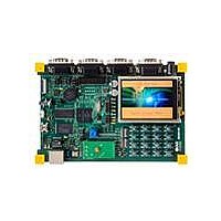
KIT DEVELOPMENT I.MX257, ARM926
Manufacturer
Freescale Semiconductor
Series
i.MX25r
Type
MCUr
Datasheets
1.MCIMX25WPDKJ.pdf
(2 pages)
2.IAR-KSK-IMX25.pdf
(154 pages)
3.IAR-KSK-IMX25.pdf
(2 pages)
4.IAR-KSK-IMX25.pdf
(57 pages)
Specifications of IAR-KSK-IMX25
Contents
Board, Cables, CD, Debugger, Power Supply
Processor To Be Evaluated
I.MX257
Processor Series
i.MX25
Data Bus Width
16 bit
Interface Type
UART, JTAG, USB, Ethernet, SD/MMC
Core
ARM926EJ-S
Silicon Manufacturer
Freescale
Core Architecture
ARM
Core Sub-architecture
ARM9
Silicon Core Number
I.MX2
Silicon Family Name
I.MX25
Mcu Supported Families
I.MX25
For Use With/related Products
i.MX25
Lead Free Status / RoHS Status
Lead free / RoHS Compliant


3.7.6.2
The i.MX25 NFC supports normal timing mode, using two Flash clock cycles for one access of RE and
WE. AC timings are provided as multiplications of the clock cycle and fixed delay.
Figure 37
under normal mode.
68
2
3
SDRAM CLK and DQS-related parameters are measured from the 50% point. That is, high is defined as 50% of the signal
value, and low is defined as 50% of the signal value. DDR SDRAM CLK parameters are measured at the crossing point of
SDCLK and SDCLK (inverted clock).
The value was calculated for an SDCLK frequency of 133 MHz, by the formula tQH = tHP – tQHS = min. (tCL,tCH) – tQHS =
0.45*tCK – tQHS = 0.45 * 7.5 – 0.45 = 2.925 ns
depicts the relative timing between NFC signals at the module level for different operations
NAND Flash Controller (NFC) Timing
NFCE
NFIO[7:0]
NFWE
NFCLE
NFWE
NFALE
NFCE
NFCLE
NFIO[7:0]
NFALE
i.MX25 Applications Processor for Consumer and Industrial Products, Rev. 8
Table 55
Figure 34. Command Latch Cycle Timing Diagram
Figure 35. Address Latch Cycle Timing Diagram
describes the timing parameters (NF1–NF17) that are shown in the figures.
NF6
NF6
NF3
NF3
NF1
NF1
Command
NF8
Address
NF5
NF8
NF5
NF10
NF4
NF9
NF7
NF9
NF7
NF11
NF2
NF4
Figure 34
Freescale Semiconductor
through
Related parts for IAR-KSK-IMX25
Image
Part Number
Description
Manufacturer
Datasheet
Request
R

Part Number:
Description:
Manufacturer:
Freescale Semiconductor, Inc
Datasheet:
Part Number:
Description:
Manufacturer:
Freescale Semiconductor, Inc
Datasheet:
Part Number:
Description:
Manufacturer:
Freescale Semiconductor, Inc
Datasheet:
Part Number:
Description:
Manufacturer:
Freescale Semiconductor, Inc
Datasheet:
Part Number:
Description:
Manufacturer:
Freescale Semiconductor, Inc
Datasheet:
Part Number:
Description:
Manufacturer:
Freescale Semiconductor, Inc
Datasheet:
Part Number:
Description:
Manufacturer:
Freescale Semiconductor, Inc
Datasheet:
Part Number:
Description:
Manufacturer:
Freescale Semiconductor, Inc
Datasheet:
Part Number:
Description:
Manufacturer:
Freescale Semiconductor, Inc
Datasheet:
Part Number:
Description:
Manufacturer:
Freescale Semiconductor, Inc
Datasheet:
Part Number:
Description:
Manufacturer:
Freescale Semiconductor, Inc
Datasheet:
Part Number:
Description:
Manufacturer:
Freescale Semiconductor, Inc
Datasheet:
Part Number:
Description:
Manufacturer:
Freescale Semiconductor, Inc
Datasheet:
Part Number:
Description:
Manufacturer:
Freescale Semiconductor, Inc
Datasheet:
Part Number:
Description:
Manufacturer:
Freescale Semiconductor, Inc
Datasheet: