IAR-KSK-IMX25 Freescale Semiconductor, IAR-KSK-IMX25 Datasheet - Page 25
IAR-KSK-IMX25
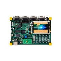
Manufacturer Part Number
IAR-KSK-IMX25
Description
KIT DEVELOPMENT I.MX257, ARM926
Manufacturer
Freescale Semiconductor
Series
i.MX25r
Type
MCUr
Datasheets
1.MCIMX25WPDKJ.pdf
(2 pages)
2.IAR-KSK-IMX25.pdf
(154 pages)
3.IAR-KSK-IMX25.pdf
(2 pages)
4.IAR-KSK-IMX25.pdf
(57 pages)
Specifications of IAR-KSK-IMX25
Contents
Board, Cables, CD, Debugger, Power Supply
Processor To Be Evaluated
I.MX257
Processor Series
i.MX25
Data Bus Width
16 bit
Interface Type
UART, JTAG, USB, Ethernet, SD/MMC
Core
ARM926EJ-S
Silicon Manufacturer
Freescale
Core Architecture
ARM
Core Sub-architecture
ARM9
Silicon Core Number
I.MX2
Silicon Family Name
I.MX25
Mcu Supported Families
I.MX25
For Use With/related Products
i.MX25
Lead Free Status / RoHS Status
Lead free / RoHS Compliant


1. Simulation circuit for parameters Voh and Vol for I/O cells is below
2. Hysteresis of 250 mV is guaranteed over all operating conditions when hysteresis is enabled.
3. Minimum condition: bcs model, OVDD = 3.6 V / 1.95 V and –40 °C. Typical condition: typical model, OVDD = 3.3 V / 1.8 V, and
4. Typical condition: typical model, OVDD=3.3 V / 1.8 V, and 25 °C. Maximum condition: bcs model, OVDD=3.6 V / 1.95 V, and
3.6
This section provides the AC parameters for slow and fast I/O.
Figure 3
propagation waveforms.
Freescale Semiconductor
Input current (47 kΩ PU)
Input current (100 kΩ PU)
Input current (100 kΩ PD)
High-impedance I/O supply current Icc–ovdd
High-impedance core supply current Icc–vddi
25 °C. Maximum condition: wcs model, OVDD = 3.0 V, and 105 °C.
105 °C.
DC Electrical Characteristics
shows the load circuit for output.
AC Electrical Characteristics
i.MX25 Applications Processor for Consumer and Industrial Products, Rev. 8
Table 20. GPIO DC Electrical Characteristics (continued)
Symbol
IIN
IIN
IIN
CL includes package, probe and jig capacitance
Figure 3. Load Circuit for Output
From Output
VI = 0, OVDD = 3.3 V
VI = 0, OVDD = 1.8 V
VI = 0, OVDD = 3.3 V
VI = 0, OVDD = 1.8 V
VI = 0, OVDD = 3.3 V
VI = 0, OVDD = 1.8 V
VI = 0, OVDD = 3.3 V
VI = 0, OVDD = 1.8 V
VI = 0, OVDD = 3.3 V
VI = 0, OVDD = 1.8 V
Under Test
VI = OVDD = 3.3 V
VI = OVDD = 1.8 V
VI = OVDD = 3.3 V
VI = OVDD = 1.8 V
VI = OVDD = 3.3 V
VI = OVDD = 1.8 V
VI = OVDD = 3.3 V
VI = OVDD = 1.8 V
VI = OVDD = 3.3 V
VI = OVDD = 1.8 V
Test Conditions
Figure 4
through
Test Point
CL
Figure 6
0.0001
0.0001
0.0001
0.0001
0.0001
0.0001
Min.
54
30
25
14
25
14
—
—
show the output transition time and
Typ.
—
—
—
—
—
0.0001
0.0001
0.0001
0.0001
0.0001
0.001
Max.
688
688
560
560
490
490
410
410
88
49
42
23
42
23
Units Notes
μA
μA
μA
nA
nA
4
4
25
Related parts for IAR-KSK-IMX25
Image
Part Number
Description
Manufacturer
Datasheet
Request
R

Part Number:
Description:
Manufacturer:
Freescale Semiconductor, Inc
Datasheet:
Part Number:
Description:
Manufacturer:
Freescale Semiconductor, Inc
Datasheet:
Part Number:
Description:
Manufacturer:
Freescale Semiconductor, Inc
Datasheet:
Part Number:
Description:
Manufacturer:
Freescale Semiconductor, Inc
Datasheet:
Part Number:
Description:
Manufacturer:
Freescale Semiconductor, Inc
Datasheet:
Part Number:
Description:
Manufacturer:
Freescale Semiconductor, Inc
Datasheet:
Part Number:
Description:
Manufacturer:
Freescale Semiconductor, Inc
Datasheet:
Part Number:
Description:
Manufacturer:
Freescale Semiconductor, Inc
Datasheet:
Part Number:
Description:
Manufacturer:
Freescale Semiconductor, Inc
Datasheet:
Part Number:
Description:
Manufacturer:
Freescale Semiconductor, Inc
Datasheet:
Part Number:
Description:
Manufacturer:
Freescale Semiconductor, Inc
Datasheet:
Part Number:
Description:
Manufacturer:
Freescale Semiconductor, Inc
Datasheet:
Part Number:
Description:
Manufacturer:
Freescale Semiconductor, Inc
Datasheet:
Part Number:
Description:
Manufacturer:
Freescale Semiconductor, Inc
Datasheet:
Part Number:
Description:
Manufacturer:
Freescale Semiconductor, Inc
Datasheet: