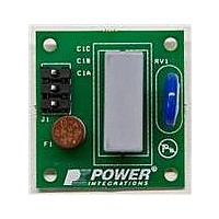
RDK-252 Power Integrations, RDK-252 Datasheet - Page 4

RDK-252
Manufacturer Part Number
RDK-252
Description
KIT REF DESIGN DG CAPZERO
Manufacturer
Power Integrations
Series
CAPZero™r
Type
Other Power Managementr
Specifications of RDK-252
Main Purpose
Automatic X Capacitor Discharge
Embedded
No
Utilized Ic / Part
CAP014DG, CAP002DG, CAP012DG
Primary Attributes
Low No-Load Input Power (
Secondary Attributes
Surge Testing to EN6100-4-5 Class 4
Input Voltage
85 V to 264 V
Board Size
38.1 mm x 25.4 mm
Product
Power Management Modules
Dimensions
38.1 mm x 25.4 mm
Lead Free Status / RoHS Status
Lead free / RoHS Compliant
For Use With/related Products
CAP014DG
Other names
596-1313
Available stocks
Company
Part Number
Manufacturer
Quantity
Price
Company:
Part Number:
RDK-252
Manufacturer:
Power Integrations
Quantity:
135
Nominal Output Voltage, V
Enter the nominal output voltage of the main output during the
continuous load condition. Generally the main output is the
output from which feedback is derived.
Continuous / Average Output Power P
Enter the average output power of the power supply. If the
power supply is a multiple output power supply, enter the sum
total power of all the outputs.
Peak Output Power P
Enter the peak output power under peak load conditions. If the
design does not have a peak load condition, then leave this
entry blank and a value equal to P
used to calculate the primary inductance value.
In multiple output designs, the output power of the main output
(typically the output from which feedback is taken) should be
increased such that the peak power (or maximum continuous
output power as applicable) matches the sum of the output
power from all the outputs in the design. The individual output
voltages and currents should then be entered at the bottom of
the spreadsheet (cells [B122 to B168]).
Select Heatsink Type and Enclosure
The enclosure determines the maximum power capability of the
TOPSwitch-JX device. If the power supply is going to be
housed in a sealed plastic case (much like an laptop power
supply) then select the adapter enclosure. If on the other hand
the power supply has better air flow, select the open frame
enclosure.
Depending on the package selected an appropriate heatsink
type can be selected. The E package always needs an external
heatsink but a V package may be used either with or without an
external heatsink. When used without a heatsink the copper
area on the PCB provides the only heatsinking. However due to
the increased thermal resistance of the PCB, as compared to an
external heatsink, the maximum power capability in this
configuration will be reduced.
Power Supply Efficiency, h
Enter the estimated efficiency of the complete power supply
measured at the output terminals under peak load conditions
and worst-case line (generally lowest input voltage). Start with a
value of 80% for VAC
are typical for a design where the majority of the output power is
drawn from an output voltage of 12 V and no output current
sensing is present on the secondary. For a 5 V output starting
values of 75% for VAC
recommended. Once a prototype has been constructed, then
measured efficiency can be entered and a further transformer
iteration performed, as appropriate.
Rev. A 030910
Figure 4.
DC INPUT VOLTAGE PARAMETERS
VMIN
VMAX
4
Application Note
DC Input Voltage Parameters Showing Grey Override Cells for DC Input Designs.
MIN
MIN
O(PEAK)
of 85 VAC and 85% for 195 VAC. These
of 85 VAC and 80% for 195 VAC are
O
(W)
(V)
O(AVE)
is assumed. P
O(AVE)
(W)
O(PEAK)
is
375 Volts
74 Volts
Power Supply Loss Allocation Factor, Z
This factor represents the proportion of losses between the
primary and the secondary of the power supply. Z factor is
used together with the efficiency number to determine the
actual power that must be delivered by the power stage. For
example, losses in the input stage (EMI filter, rectification, etc)
are not processed by the power stage (transferred through the
transformer) and therefore, although they reduce efficiency, the
transformer design is not affected by their effect on efficiency.
Examples of primary side losses are losses incurred in the input
rectifier and EMI filter, MOSFET conduction losses and primary
side winding losses. Examples of secondary side losses include
the losses in secondary diode, secondary windings and core
losses, losses associated with the primary side clamp circuit
and the bias winding. For designs that do not have a peak power
requirement, a value of 0.5 is recommended. For designs with
a peak power requirement, enter 0.65. This difference accounts
for increased input stage losses under peak power loading
Bias Winding Output Voltage (V
Enter the voltage at the output of the bias winding output. A
starting value of 15 V is recommended. The voltage may be set
to different values, for example, when the bias winding output is
also used as a primary side (non-isolated) auxiliary output. Higher
voltages increase no-load input power while values below 8 V
are not recommended as at light load there may be insufficient
voltage to correctly bias the optocoupler, causing loss of output
regulation. A 10 µF, 50 V electrolytic capacitor is the recommended
minimum value for the bias winding output filter.
Bridge Diode Conduction Time, t
Enter a bridge diode conduction time of 3.00 ms if there is no
better data available.
Total Input Capacitance, C
Table 3 suggests suitable multiplication factors to be used for
calculating input capacitance for different AC input voltage ranges.
Table 3. Suggested Total Input Capacitance for Different Input Voltage Ranges.
The capacitance is used to calculate the minimum and
maximum DC voltage across the bulk capacitor and should be
selected to keep the minimum DC input voltage, V
AC Input Voltage (VAC)
Minimum DC Input Voltage
Maximum DC Input Voltage
100/115
85-265
230
Z =
Secondary Side Losses
Total Losses
IN
(µF)
B
Total Input Capacitance per
)
Watt Output Power (µF/W)
C
Full Wave Rectification
(ms)
2 – 3
2 – 3
www.powerint.com
1
MIN
>70 V.
AN-47


