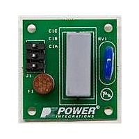
RDK-252 Power Integrations, RDK-252 Datasheet - Page 18

RDK-252
Manufacturer Part Number
RDK-252
Description
KIT REF DESIGN DG CAPZERO
Manufacturer
Power Integrations
Series
CAPZero™r
Type
Other Power Managementr
Specifications of RDK-252
Main Purpose
Automatic X Capacitor Discharge
Embedded
No
Utilized Ic / Part
CAP014DG, CAP002DG, CAP012DG
Primary Attributes
Low No-Load Input Power (
Secondary Attributes
Surge Testing to EN6100-4-5 Class 4
Input Voltage
85 V to 264 V
Board Size
38.1 mm x 25.4 mm
Product
Power Management Modules
Dimensions
38.1 mm x 25.4 mm
Lead Free Status / RoHS Status
Lead free / RoHS Compliant
For Use With/related Products
CAP014DG
Other names
596-1313
Available stocks
Company
Part Number
Manufacturer
Quantity
Price
Company:
Part Number:
RDK-252
Manufacturer:
Power Integrations
Quantity:
135
Y Capacitor
The preferred Y capacitor connection is close to the transformer
secondary output return pin(s) and the positive primary DC input
pin of the transformer. If the Y capacitor is connected between
primary and secondary RTN, then the primary connection
should be made via a dedicated trace from the Y capacitor to
the negative input capacitor terminal. This ensures that line
surge created displacement currents across the isolation barrier
are routed away from traces connected to the TOPSwitch-JX.
Rev. A 030910
Figure 19. Layout Considerations (Shown Schematically) and Common Mistakes.
Kelvin connect at
SOURCE pin, no
power currents flow
in signal traces
Without Kelvin connection
at SOURCE pin, power
current (I
drop in trace (∆V
modulates source reference
of controller
✓ Recommended Layout
✘ Poor Signal Source Connection
Line sense resistor
(R
input capacitor
R
physically
close to X pin
18
IL
LS
R
physically
close to V pin
placed
) connected at
LS
For correct device operation ensure that good layout practices are followed
placed
S
Application Note
) creates voltage
Poor layout may cause higher output ripple or prevent proper device operation
PRI RTN
B+
S
), which
PRI RTN
B+
∆V
D
S
S
R
I
S
IL
CONTROL
X
D
S
V
R
CLAMP
LS
F
CONTROL
X
C
TOPSwitch-JX
V
CLAMP
F
TOPSwitch-JX
C
PI-5764-030310
C
Y1
PI-5766-011310
C
Y1
Preferred Y capacitor
placement
(B+ to output RTN)
CONTROL pin decoupling
capacitor placed directly
between CONTROL and
SOURCE pins
Y capacitor (C
bias return connected
with dedicated trace
directly to PRI RTN
at input capacitor
C
Y2
C
Y2
Y2
) and
Secondary
To minimize leakage inductance and EMI, the area of the loop
connecting the secondary winding, the output diode and the
output filter capacitor should be minimized. In addition,
sufficient copper area should be provided at the anode and
cathode terminal of the diode for heatsinking. A larger area is
preferred at the quiet cathode terminal as a large anode area
can increase high frequency radiated EMI.
✘ Poor Line Sense Resistor Location and Connection
Poor layout may cause higher output ripple or prevent proper device operation
✘ Poor Bias Winding Return Connection
PRI RTN
R
device. Increases V pin
node area, increasing
potential noise coupling
Voltage drop across
trace impedance (∆V
modulates V pin current
LS
B+
placed away from
V pin trace routed in
close proximity to
drain node causing
noise coupling
Poor layout may cause changes in UV/OV thresholds and higher output ripple
PRI RTN
D
S
B+
B+
)
CONTROL
X
V
CLAMP
∆V
F
TOPSwitch-JX
S
I
B+
∆V
C
D
S
B+
CONTROL
C
X
Y1
PI-5765-011210
V
CLAMP
R
LS
I
F
I
BIAS
CY2
TOPSwitch-JX
+
C
Bias winding return and
primary to secondary
displacement currents (via C
flow through signal traces.
Voltage drop (∆V
impedances modulates source
reference of controller
C
PI-5767-012810
Y1
C
www.powerint.com
Y2
S
) across trace
AN-47
C
Y2
Y2
)


