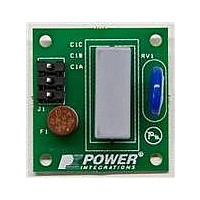
RDK-252 Power Integrations, RDK-252 Datasheet - Page 13

RDK-252
Manufacturer Part Number
RDK-252
Description
KIT REF DESIGN DG CAPZERO
Manufacturer
Power Integrations
Series
CAPZero™r
Type
Other Power Managementr
Specifications of RDK-252
Main Purpose
Automatic X Capacitor Discharge
Embedded
No
Utilized Ic / Part
CAP014DG, CAP002DG, CAP012DG
Primary Attributes
Low No-Load Input Power (
Secondary Attributes
Surge Testing to EN6100-4-5 Class 4
Input Voltage
85 V to 264 V
Board Size
38.1 mm x 25.4 mm
Product
Power Management Modules
Dimensions
38.1 mm x 25.4 mm
Lead Free Status / RoHS Status
Lead free / RoHS Compliant
For Use With/related Products
CAP014DG
Other names
596-1313
Available stocks
Company
Part Number
Manufacturer
Quantity
Price
Company:
Part Number:
RDK-252
Manufacturer:
Power Integrations
Quantity:
135
Figure 13a shows an example of an RCD + Zener clamp. During
normal operation the Zener diode does not conduct, clamping is
provided by R
optimized for full load rather than overload and start-up. This
results in lower dissipation and improved light load and no-load
input power. During output overload and start-up VR
provides a defined maximum drain voltage below the BV
rating of the MOSFET. In high power designs, multiple Zeners
may be required to share dissipation, shown in gray in Figure 13a.
A Zener clamp may also be used (R
which results in excellent full load and light efficiency plus low
no-load input power but higher EMI.
Figure 13b shows an efficient RCDZ clamp circuit. This
configuration provides the light load and no-load performance of
Figure 14. Typical Zener Feedback Circuit.
Figure 15. Optocoupler-TL431 Feedback Circuit.
www.powerint.com
AN-47
CLAMP
and C
+
V
+
AC
V
AC
CLAMP
* 47 Ω is suitable for V
**470 Ω is good for Zeners with I
Optional
Optional
. This allows the values to be
CLAMP
C
C
IN
O
IN
D
and C
S
D
upto 7.5 V. For V
S
CONTROL
CONTROL
X
ZT
CLAMP
X
V
= 5 mA. Lower values are needed for Zeners with higher I
V
F
100 nF
TOPSwitch-JX
F
100 nF
TOPSwitch-JX
are eliminated)
O
C
>7.5 V, a higher value may be required for optimum transient response.
C
CLAMP
DSS
6.8 Ω
47 µF
6.8 Ω
47 µF
the Zener clamp as well as the low EMI characteristic of an RCD
clamp. The benefit of this circuit is that at light load or no-load
C
normal RCD clamp at light or no-load the capacitor ripple
voltage becomes very large (>V
giving poor no-load input power and low light load efficiency.
The operation is similar to the traditional RCD clamp. After the
turn-off event of the switch, capacitor C
R
turn-off event. Dissipation is shared between VR
R
components. The recommended value for VR
10% higher than the V
placed in series to increase the power capability of the Zeners.
TL431
CLAMP
CLAMP
CLAMP
C
B
R
B
100 Ω
does not discharge below the value of VR
and VR
in proportion to the voltages across these two
Zener
200 Ω (V
1 kΩ (V
R
LTV817A
3.3 kΩ
R
2%
UTV817A
D
D
D
R
Feedback Circuit
Z
T
∗
L
L
PF
O
PF
470 Ω
ZT
O
= 12 V)
R
. (E.g. 150 Ω for I
100 nF
CLAMP
10 kΩ
= 5 V)
BIAS
R
C
R
S2
T
∗∗
S1
, resetting the capacitor ready for the next
OR
C
C
PF
PF
ZT
of the design. Two Zeners can be
CIRCUIT PERFORMANCE
Circuit Tolerance ±5%
Load Regulation ±1%
Line Regulation ±0.5%
= 20 mA).
CIRCUIT PERFORMANCE
Circuit Tolerance ±1%
Load Regulation ±0.2%
Line Regulation ±0.2%
R =
PI-5763-012810
PI-5762-022210
Feedback Circuit
V
V
V
+
-
O
+
-
O
O
Application Note
OR
2.5
- 2.5
) and the clamp the main load
X 10 kΩ
CLAMP
is discharged via
CLAMP
CLAMP
CLAMP
is about
. In a
and
Rev. A 030910
13


