RDK-201 Power Integrations, RDK-201 Datasheet
RDK-201
Specifications of RDK-201


Related parts for RDK-201


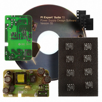
RDK-201 Summary of contents
Page 1
LNK623-626 LinkSwitch-CV Family ® Energy-Effi cient, Off-line Switcher with Accurate Primary-side Constant-Voltage (CV) Control Product Highlights Dramatically Simplifi Converters Eliminates optocoupler and all secondary CV control circuitry • Eliminates bias winding supply – self biasing • ...
Page 2
LNK623-626 BYPASS (BP) + FEEDBACK (FB) t SAMPLE-OUT FB 6 MAX I SOURCE LIM (S) Figure 2 Functional Block Diagram. Pin Functional Description DRAIN (D) Pin: This pin is the power MOSFET drain connection. It ...
Page 3
LinkSwitch-CV Functional Description The LinkSwitch-CV combines a high voltage power MOSFET switch with a power supply controller in one device. Similar to the LinkSwitch-LP and TinySwitch-III it uses ON/OFF control to regulate the output voltage. The LinkSwitch-CV controller consists of ...
Page 4
... DC is fi ltered by the bulk storage capacitors C1 and C2. Inductor L1, L2, C1 and C2 form a pi (π) fi lter, which attenuates conducted differential-mode EMI noise. This confi guration along with Power Integrations transformer E-shield ™ technology allow this design to meet EMI standard EN55022 class B with good margin without requiring a Y capacitor ...
Page 5
Output Regulation The LNK626 regulates the output using ON/OFF control, enabling or disabling switching cycles based on the sampled voltage on the FEEDBACK pin. The output voltage is sensed using a primary referenced winding on transformer T1 eliminating the need ...
Page 6
LNK623-626 Primary Side Input Filter Capacitor C1 Copper area L1 maximized for heatsinking RV1 RT1 J1 10 mil gap IN Figure 5. PCB Layout Example. B+ CLAMP Minimize FB PRI RTN ...
Page 7
B+ Power currents flow in signal source trace Trace impedance PRI RTN Voltage drops across trace impedance Figure 8. Schematic Representation of Electrical Impact of Improper Layout. www.powerint.com CLAMP Drain trace in close proximity of feedback trace will couple noise ...
Page 8
LNK623-626 Drain Clamp Recommended Clamp Circuits PI-5107-110308 Figure 9. RCD Clamp, Low Power or Low Leakage Inductance Designs. Components R1, R2, C3, VR1 and D5 in fi gure 4 comprise the clamp. ...
Page 9
Clampless Designs Clampless designs rely solely on the drain node capacitance to limit the leakage inductance induced peak drain-to-source voltage. Therefore the maximum AC input line voltage, the value the leakage inductance energy, (a function of leakage ...
Page 10
... Enough thermal margin should be allowed for the part-to-part variation of the R specifi the data sheet recommended that the maximum source pin temperature does not exceed 110 °C. Design Tools Up-to-date information on design tools can be found at the Power Integrations web site: www.powerint.com of LinkSwitch-CV, as DS(ON) www.powerint.com ...
Page 11
Absolute Maximum Ratings DRAIN Voltage .................................. ......... ..............-0 700 V DRAIN Peak Current: LNK623 ......................... 400 (600) mA LNK624 ......................... 400 (600) mA LNK625 ..........................528 (790) mA LNK626 ........................720 (1080) mA Peak Negative Pulsed DRAIN Current ................... ...
Page 12
LNK623-626 Parameter Symbol Control Functions (cont.) Minimum Switch t “On”-Time ON(min) Feedback Pin t Sampling Delay DRAIN Supply Current CH1 BYPASS Pin Charge Current I CH2 BYPASS Pin V Voltage BP BYPASS Pin V ...
Page 13
Parameter Symbol Output ON-State R Resistance DS(ON) I DSS1 OFF-State Leakage I DSS2 Breakdown BV Voltage DSS DRAIN Supply Voltage Auto-Restart t ON-Time AR-ON Auto-Restart t OFF-Time AR-OFF Open-Loop FB Pin I Current Threshold OL Open-Loop ON-Time NOTES ...
Page 14
LNK623-626 Typical Performance Characteristics 1.200 1.000 0.800 0.600 0.400 0.200 0.000 -40 - Temperature (°C) Figure 13. Output Frequency vs, Temperature. 1.1 1.0 0.9 -50 - Junction Temperature (°C) Figure 15. Breakdown vs. Temperature. 1000 ...
Page 15
Raise V voltage from 6.2 V, down Raise V until cycle skipping occurs Apply 1 and measure ...
Page 16
LNK623-626 ⊕ .004 (.10) -E- .240 (6.10) .260 (6.60) Pin 1 .367 (9.32) -D- .387 (9.83) .125 (3.18) .145 (3.68) -T- SEATING PLANE .100 (2.54) BSC .048 (1.22) .053 (1.35) .014 (.36) ⊕ .010 ...
Page 17
B 4 4.90 (0.193) BSC A 8 3.90 (0.154) BSC 2 0.10 (0.004 Pin 1 ID 1.27 (0.050) BSC 1.25 - 1.65 1.35 (0.053) 1.75 (0.069) (0.049 - 0.065) 0.10 (0.004) 0.25 (0.010) Reference Solder Pad ...
Page 18
... The products and applications illustrated herein (including transformer construction and circuits external to the products) may be covered by one or more U.S. and foreign patents, or potentially by pending U.S. and foreign patent applications assigned to Power Integrations. A complete list of Power Integrations patents may be found at www.powerint.com. Power Integrations grants its customers a license under certain patent rights as set forth at http://www ...