RDK-252 Power Integrations, RDK-252 Datasheet - Page 19
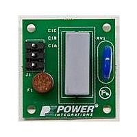
RDK-252
Manufacturer Part Number
RDK-252
Description
KIT REF DESIGN DG CAPZERO
Manufacturer
Power Integrations
Series
CAPZero™r
Type
Other Power Managementr
Specifications of RDK-252
Main Purpose
Automatic X Capacitor Discharge
Embedded
No
Utilized Ic / Part
CAP014DG, CAP002DG, CAP012DG
Primary Attributes
Low No-Load Input Power (
Secondary Attributes
Surge Testing to EN6100-4-5 Class 4
Input Voltage
85 V to 264 V
Board Size
38.1 mm x 25.4 mm
Product
Power Management Modules
Dimensions
38.1 mm x 25.4 mm
Lead Free Status / RoHS Status
Lead free / RoHS Compliant
For Use With/related Products
CAP014DG
Other names
596-1313
Available stocks
Company
Part Number
Manufacturer
Quantity
Price
Company:

Part Number:
RDK-252
Manufacturer:
Power Integrations
Quantity:
135


Figure 20. Primary Sensed OVP circuit for TOPSwitch-JX Based Flyback
Figure 22. Implementation of Overvoltage Protection Together With Over-Power
Common Layout Problems to Avoid
A poor layout will often result in performance issues that may
be time consuming to analyze, and they may occur at the end
of development, when PCB design changes are difficult.
Figure 19 will help quickly identify the root cause of a problem
and correct the layout. The figure schematically shows common
layout mistakes and the reasons they should be avoided
Light Load Efficiency and No-load Input Power
Hints and Tips
Correct Power Meter Configuration
Figure 25 shows the two possible configurations for the voltage
and current sense elements in a power meter and their typical
impedances. The individual voltage and current elements are
Figure 21. Primary Sensed Overvoltage Protection Circuit for a Flyback
www.powerint.com
AN-47
D
S
D
S
D
S
R
CONTROL
CONTROL
Power Supply.
Protection Using the TOPSwitch-JX
Power Supply Using TOPSwitch-JX with Additional V Pin
Noise Decoupling.
CONTROL
LS
V
V
X
X
V
X
1N4148
F
F
F
C
1N4148
C
C
R
OVP
R
OPP
R
100 nF
VR
VR
1 MΩ
R
OVP
OVP
OPP
OVP
VR
VR
OVP
OVP
C
R
P
0 to 47 Ω
P
R
R
PI-4822-022008
PI-5824-020210
BIAS
BIAS
PI-4821-022008
C
D
B
B
typically brought out onto the rear of the instrument allowing
user configuration.
For low power measurements (<100 W) configuration (a) should
be used. This prevents the static loss from the input impedance
of the voltage sense element being included in the power readings.
At 230 VAC this equals an error of 26 mW for a meter with 2 MW
input impedance. This fails to meet the ≤0.01 W uncertainty
requirement of most energy efficiency test methods (IEC 62301)
when measuring no-load input power. Configuration (a) does
introduce an error due to the voltage drop (power dissipation)
across the current sense element. However for low current
measurements this is typically negligible. For example for an
85 VAC, 2 A
power measurement error of <0.05% vs. the ≤2% requirement.
A quick check to see if the power meter is correctly configured
is to apply 230 VAC to the power meter with no power supply
unit (PSU) connected. If the power meter displays a non-zero
power value then it is likely that configuration (b) is being used.
Switch the power meter to configuration (a).
Figure 23. Biasing the V Pin from C Pin Allows for Lower No-load Power
Figure 24. Use of Darlington Pair to Reduce No-load Input Power.
TOPSwitch-JX
Transformer
DC BUS
To
Consumption.
R
R
TOPSwitch-JX
RMS
LS1
LS2
D
S
Transformer
measurement the dissipation is 64 mW giving a
CONTROL
To
X
V
R
F
DC BUS
LS1
D
S
To
, R
C
LS2
CONTROL
0.1 µF
Application Note
X
V
F
6.8 Ω
47 µF
C
2N2222
20 Ω
Q
PI-5768-011410
X
0.1 µF
PI-5769-030510
R
CV
Winding
Bias
20 Ω
To
6.8 Ω
47 µF
Rev. A 030910
PC817A
19
Related parts for RDK-252
Image
Part Number
Description
Manufacturer
Datasheet
Request
R

Part Number:
Description:
KIT REF DESIGN TOP HX FOR TOP258
Manufacturer:
Power Integrations
Datasheet:

Part Number:
Description:
KIT REF DESIGN LINKSWITCH 2
Manufacturer:
Power Integrations
Datasheet:

Part Number:
Description:
KIT REF DESIGN 1.2W PS TN FAMILY
Manufacturer:
Power Integrations
Datasheet:

Part Number:
Description:
KIT REF DESIGN 36-72W MOTOR DRVR
Manufacturer:
Power Integrations
Datasheet:

Part Number:
Description:
KIT REF DESIGN FOR LNK457D
Manufacturer:
Power Integrations
Datasheet:

Part Number:
Description:
REFERENCE DESIGN LINKSWITCH-PH
Manufacturer:
Power Integrations
Datasheet:

Part Number:
Description:
Specifications: Manufacturer: Power Integrations ; Output Voltage: 380 VDC ; Input / Supply Voltage (Max): 264 VAC ; Input / Supply Voltage (Min): 90 VAC ; Mounting Style: Through Hole ; Output Current: 0.913 A ; Output Power: 347 W
Manufacturer:
Power Integrations, Inc.

Part Number:
Description:
Power Management Modules & Development Tools TOPSwitch-JX REF. DESIGN KIT
Manufacturer:
Power Integrations
Datasheet:
Part Number:
Description:
Power Management IC Development Tools REF DESIGN RDR-292 PFF LED STREET LIGHT
Manufacturer:
Power Integrations

Part Number:
Description:
KIT REF DESIGN FOR LNK403EG
Manufacturer:
Power Integrations
Datasheet:

Part Number:
Description:
KIT REF DESIGN FOR LNK406EG
Manufacturer:
Power Integrations
Datasheet:

Part Number:
Description:
KIT REF DESIGN LINKSWITCH-CV
Manufacturer:
Power Integrations
Datasheet:

Part Number:
Description:
KIT REF DESIGN PFS762HG
Manufacturer:
Power Integrations
Datasheet:
Part Number:
Description:
Specifications: Family: Eval Boards - DC/DC & AC/DC (Off-Line) SMPS ; Series: HiperLCS™ ; Main Purpose: DC/DC, Step Down ; Outputs and Type: 1, Isolated ; Power - Output: 150W ; Voltage - Output: 24V ; Current - Output: 6.25A ; Voltage - Input:
Manufacturer:
Power Integrations, Inc.
Datasheet:

Part Number:
Description:
KIT REFERENCE DESIGN W/TN376PN
Manufacturer:
Power Integrations
Datasheet: