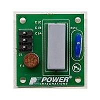
RDK-252 Power Integrations, RDK-252 Datasheet - Page 25

RDK-252
Manufacturer Part Number
RDK-252
Description
KIT REF DESIGN DG CAPZERO
Manufacturer
Power Integrations
Series
CAPZero™r
Type
Other Power Managementr
Specifications of RDK-252
Main Purpose
Automatic X Capacitor Discharge
Embedded
No
Utilized Ic / Part
CAP014DG, CAP002DG, CAP012DG
Primary Attributes
Low No-Load Input Power (
Secondary Attributes
Surge Testing to EN6100-4-5 Class 4
Input Voltage
85 V to 264 V
Board Size
38.1 mm x 25.4 mm
Product
Power Management Modules
Dimensions
38.1 mm x 25.4 mm
Lead Free Status / RoHS Status
Lead free / RoHS Compliant
For Use With/related Products
CAP014DG
Other names
596-1313
Available stocks
Company
Part Number
Manufacturer
Quantity
Price
Company:
Part Number:
RDK-252
Manufacturer:
Power Integrations
Quantity:
135
Appendix A
Application Example
Low No-load, High Efficiency, 65 W, Universal Input
Adapter Power Supply
The circuit shown in Figure 31 shows a 90 VAC to 265 VAC
input, 19 V, 3.42 A output power supply, designed for operation
inside a sealed adapter case type. The goals of the design were
highest full load efficiency, highest average efficiency (average of
25%, 50%, 75% and 100% load points), and very low no-load
consumption. Additional requirements included latching output
overvoltage shutdown and compliance to safety agency limited
power source (LPS) limits. Measured efficiency and no-load
performance is summarized in the table shown in the schematic
which easily exceed current energy efficiency requirements.
In order to meet these design goals the following key design
decisions were made.
PI Part Selection
•
The current limit programming feature of TOPSwitch-JX allows
the selection of a larger device than needed for power delivery.
This gives higher full load, low line efficiency by reducing the
MOSFET conduction losses (I
overload power, transformer and other components size as if a
smaller device had been used.
For this design one device size larger than required for power
delivery (as recommended by the power table) was selected.
Figure 31. Schematic of High-Efficiency 19 V, 65 W, Universal Input Flyback Supply With Low No-Load.
www.powerint.com
AN-47
One device size larger selected than required for power
delivery to increase efficiency.
L
N
90 - 265
VAC
4 A
200 µH
12 mH
F1
L3
L4
2.2 MΩ
R1
No-load Input Power (mW)
275 VAC
Full Power Efficiency (%)
330 nF
Average Efficiency (%)
Input Voltage (VAC)
C1
2.2 MΩ
GBU8J
600 V
R2
D1
120 µF
400 V
C2
86.6
57.7
90
RMS
88.4
89.8
59.7
115
5.1 MΩ
5.1 MΩ
11 kΩ
2
R3
R4
1%
R9
× R
89.1
89.5
86.7
230
10 MΩ
10 MΩ
DS(ON)
R7
R8
) but maintains the
2.2 Ω
R24
2.2 nF
1 kV
SMAJ250A
C5
TOPSwitch-JX
VR2
TOP269EG
100 kΩ
R5
U1
D
S
150 Ω
1000 pF
RS1K
R6
CONTROL
630 V
D2
C4
X
V
BAV19WS
191 kΩ
F
D3
R20
1%
C
MMBT4403
220 nF
This typically gives the highest efficiency. Further increases in
device size often results in the same or lower efficiency due to
the larger switching losses associated with a larger MOSFET.
Line Sense Resistor Values
•
Line sensing is provided by resistors R3 and R4 and sets the
line undervoltage and overvoltage thresholds. The combined
value of these resistors was increased from the standard 4 MW
to 10.2 MW. This reduced the resistor dissipation, and therefore
contribution to no-load input power, from ~26 mW to ~10 mW. To
compensate the resultant change in the UV (turn-on) threshold
resistor R20 was added between the CONTROL and VOLTAGE-
MONITOR pins. This adds a DC current equal to ~16 µA into the
V pin, requiring only 9 µA to be provided via R3 and R4 to reach
the V pin UV (turn-on) threshold current of 25 µA and setting the
UV threshold to 95 VDC.
This technique does effectively disable the line OV feature as
the resultant OV threshold is raised from ~450 VDC to ~980 VDC.
However in this design there was no impact as the value of
input capacitance (C2) was sufficient to allow the design to
withstand differential line surges greater than 2 kV without the
peak drain voltage reaching the BV
Clamp Configuration – RZCD vs. RCD
•
The clamp network is formed by VR2, C4, R5, R6, and D2. It
limits the peak drain voltage spike caused by leakage
inductance to below the BV
25 V
Q1
C9
3
1
100 nF
50 V
250 VAC
Increasing line sensing resistance from 4 MW to 10.2 MW to
reduce no-load input power dissipation by 16 mW.
An RZCD (Zener bleed) was selected over an RCD clamp to
give higher light load efficiency and lower no-load consumption.
C6
RM10 FL1
C11
1 nF
T1
FL2
5
4
BAV21WS-
ZMM5244B-7
20 Ω
R14
7-F
4.7 kΩ
D4
R12
VR1
1/8 W
1/8 W
6.8 Ω
47 µF
20 Ω
R13
R25
16 V
C7
470 pF
50 V
C15
100 V
1 nF
C12
V30100C
100 Ω
MMBT3904
PS2501-
R10
56 µF
1-H-A
C10
35 V
U3B
D5
Q2
33 Ω
R15
470 µF
25 V
C13
DSS
100 nF
50 V
C22
PS2501-
1-H-A
470 µF
U3A
25 V
C14
rating of the internal TOPSwitch-
Application Note
20 kΩ
R16
DSS
LMV431AIMF
22 nF
50 V
rating of U1.
C16
U2
1%
10 kΩ
1.6 kΩ
R27
6.8 nF
147 kΩ
R22
C19
50 V
20 kΩ
R17
1%
R19
PI-5842-030810
10 kΩ
R18
1%
10 nF
50 V
C21
19 V, 3.42 A
Rev. A 030910
RTN
25


