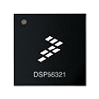
XC56309VL100A Freescale Semiconductor, XC56309VL100A Datasheet - Page 96

XC56309VL100A
Manufacturer Part Number
XC56309VL100A
Description
IC DSP 24BIT 100MHZ 196-MAPBGA
Manufacturer
Freescale Semiconductor
Series
DSP563xxr
Type
Fixed Pointr
Specifications of XC56309VL100A
Interface
Host Interface, SSI, SCI
Clock Rate
100MHz
Non-volatile Memory
ROM (576 B)
On-chip Ram
24kB
Voltage - I/o
3.30V
Voltage - Core
3.30V
Operating Temperature
-40°C ~ 100°C
Mounting Type
Surface Mount
Package / Case
196-MAPBGA
Device Core Size
24b
Format
Fixed Point
Clock Freq (max)
100MHz
Mips
100
Device Input Clock Speed
100MHz
Ram Size
102KB
Operating Supply Voltage (typ)
3.3V
Operating Supply Voltage (min)
3V
Operating Supply Voltage (max)
3.6V
Operating Temp Range
-40C to 100C
Operating Temperature Classification
Industrial
Mounting
Surface Mount
Pin Count
196
Package Type
MA-BGA
Lead Free Status / RoHS Status
Lead free / RoHS Compliant
Available stocks
Company
Part Number
Manufacturer
Quantity
Price
Company:
Part Number:
XC56309VL100A
Manufacturer:
Freescale Semiconductor
Quantity:
10 000
Company:
Part Number:
XC56309VL100AR2
Manufacturer:
Freescale Semiconductor
Quantity:
10 000
- Current page: 96 of 284
- Download datasheet (4Mb)
Programming the Peripherals
Configuring interrupts requires two steps:
Events that change bits in the peripheral control registers can then trigger the interrupt.
Depending on the peripheral, from two to six peripheral interrupt sources are available to the
programmer.
Example 5-2 shows a short interrupt programmed for the HI08. The main program enables the
Host Receive Interrupt in the Host Control Register (HCR). When the interrupt is triggered
during code execution, the core processing jumps to the Host Receive Interrupt routine location
at p:$60 and executes the code there. Since this is a short interrupt, the core returns to normal
code execution after executing the two move instructions, and an RTI instruction is not
necessary.
; Short Interrupt Routine
5.4.3 DMA
The Direct Memory Access (DMA) controller permits data transfers between internal/external
memory and/or internal/external I/O in any combination without the intervention of the
DSP56309 core. Dedicated DMA address and data buses and internal memory partitioning
ensure that a high level of isolation is achieved so the DMA operation does not interfere with the
core operation or slow it down. The DMA moves data to/from the peripheral transmit/receive
registers. The programmer can use the DMA control registers to configure sources and
destinations of data transfers. Depending on the peripheral, one to four peripheral request sources
are available. This is the most efficient method of data transfer available. Core intervention is not
required after the DMA channel is initialized.
5-4
1.
2.
bset#M_HRIE,x:M_HCR ; enable host receive interrupt
orgP:$60
movepx:M_HRX,x1
movex1,y:(r0)+
Setting up the interrupt routine
a.
b.
Enabling the interrupts
a.
b.
c.
The interrupt handler is located at the interrupt starting address.
The interrupt routines can be short (only two opcodes long) or long (more than two
opcodes and requiring a JSR instruction).
Set the corresponding bits in the applicable peripheral control register.
Enable peripheral interrupts in the Interrupt Priority Register (IPRP).
Enable global interrupts in the Mode Register (MR) portion of the Status Register
(SR).
; HI08 Receive Data Full interrupt
DSP56309 User’s Manual, Rev. 1
Example 5-2. Interrupts
Freescale Semiconductor
Related parts for XC56309VL100A
Image
Part Number
Description
Manufacturer
Datasheet
Request
R
Part Number:
Description:
Manufacturer:
Freescale Semiconductor, Inc
Datasheet:
Part Number:
Description:
Manufacturer:
Freescale Semiconductor, Inc
Datasheet:
Part Number:
Description:
Manufacturer:
Freescale Semiconductor, Inc
Datasheet:
Part Number:
Description:
Manufacturer:
Freescale Semiconductor, Inc
Datasheet:
Part Number:
Description:
Manufacturer:
Freescale Semiconductor, Inc
Datasheet:
Part Number:
Description:
Manufacturer:
Freescale Semiconductor, Inc
Datasheet:
Part Number:
Description:
Manufacturer:
Freescale Semiconductor, Inc
Datasheet:
Part Number:
Description:
Manufacturer:
Freescale Semiconductor, Inc
Datasheet:
Part Number:
Description:
Manufacturer:
Freescale Semiconductor, Inc
Datasheet:
Part Number:
Description:
Manufacturer:
Freescale Semiconductor, Inc
Datasheet:
Part Number:
Description:
Manufacturer:
Freescale Semiconductor, Inc
Datasheet:
Part Number:
Description:
Manufacturer:
Freescale Semiconductor, Inc
Datasheet:
Part Number:
Description:
Manufacturer:
Freescale Semiconductor, Inc
Datasheet:
Part Number:
Description:
Manufacturer:
Freescale Semiconductor, Inc
Datasheet:
Part Number:
Description:
Manufacturer:
Freescale Semiconductor, Inc
Datasheet:


