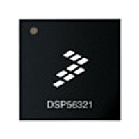
XC56309VL100A Freescale Semiconductor, XC56309VL100A Datasheet - Page 142

XC56309VL100A
Manufacturer Part Number
XC56309VL100A
Description
IC DSP 24BIT 100MHZ 196-MAPBGA
Manufacturer
Freescale Semiconductor
Series
DSP563xxr
Type
Fixed Pointr
Specifications of XC56309VL100A
Interface
Host Interface, SSI, SCI
Clock Rate
100MHz
Non-volatile Memory
ROM (576 B)
On-chip Ram
24kB
Voltage - I/o
3.30V
Voltage - Core
3.30V
Operating Temperature
-40°C ~ 100°C
Mounting Type
Surface Mount
Package / Case
196-MAPBGA
Device Core Size
24b
Format
Fixed Point
Clock Freq (max)
100MHz
Mips
100
Device Input Clock Speed
100MHz
Ram Size
102KB
Operating Supply Voltage (typ)
3.3V
Operating Supply Voltage (min)
3V
Operating Supply Voltage (max)
3.6V
Operating Temp Range
-40C to 100C
Operating Temperature Classification
Industrial
Mounting
Surface Mount
Pin Count
196
Package Type
MA-BGA
Lead Free Status / RoHS Status
Lead free / RoHS Compliant
Available stocks
Company
Part Number
Manufacturer
Quantity
Price
Company:
Part Number:
XC56309VL100A
Manufacturer:
Freescale Semiconductor
Quantity:
10 000
Company:
Part Number:
XC56309VL100AR2
Manufacturer:
Freescale Semiconductor
Quantity:
10 000
- Current page: 142 of 284
- Download datasheet (4Mb)
Enhanced Synchronous Serial Interface (ESSI)
7.4.2 Synchronous/Asynchronous Operating Modes
The transmit and receive sections of the ESSI interface are synchronous or asynchronous. The
transmitter and receiver use common clock and synchronization signals in Synchronous mode;
they use separate clock and sync signals in Asynchronous mode. The CRB[SYN] bit selects
synchronous or asynchronous operation. When the SYN bit is cleared, the ESSI TX and RX
clocks and frame sync sources are independent. If the SYN bit is set, the ESSI TX and RX clocks
and frame sync are driven by the same source (either external or internal). Since the ESSI
operates either synchronously or asynchronously, separate receive and transmit interrupts are
provided.
Transmitter 1 and transmitter 2 operate only in Synchronous mode. Data clock and frame sync
signals are generated internally by the DSP or obtained from external sources. If clocks are
internally generated, the ESSI clock generator derives bit clock and frame sync signals from the
DSP internal system clock. The ESSI clock generator consists of a selectable fixed prescaler with
a programmable prescaler for bit rate clock generation and a programmable frame-rate divider
with a word-length divider for frame-rate sync-signal generation.
7.4.3 Frame Sync Selection
The transmitter and receiver can operate independently. The transmitter can have either a bit-long
or word-long frame-sync signal format, and the receiver can have the same or another format.
The selection is made by programming the CRB FSL[1–0], FSR, and FSP bits.
7.4.4 Frame Sync Signal Format
CRB[FSL1] controls the frame sync signal format.
7.4.5 Frame Sync Length for Multiple Devices
Mixing frame sync lengths is useful in configuring systems in which data is received from one
type of device (for example, codec) and transmitted to a different type of device. CRB[FSL0]
controls whether RX and TX have the same frame sync length.
7-10
If CRB[FSL1] is cleared, the receive frame sync is asserted during the entire data transfer
period. This frame sync length is compatible with Freescale codecs, serial peripherals that
conform to the Freescale SPI, serial A/D and D/A converters, shift registers, and
telecommunication pulse code modulation serial I/O.
If CRB[FSL1] is set, the receive frame sync pulses active for one bit clock immediately
before the data transfer period. This frame sync length is compatible with Intel and
National Semiconductor Corporation components, codecs, and telecommunication pulse
code modulation serial I/O.
If CRB[FSL0] is cleared, both RX and TX have the same frame sync length.
DSP56309 User’s Manual, Rev. 1
Freescale Semiconductor
Related parts for XC56309VL100A
Image
Part Number
Description
Manufacturer
Datasheet
Request
R
Part Number:
Description:
Manufacturer:
Freescale Semiconductor, Inc
Datasheet:
Part Number:
Description:
Manufacturer:
Freescale Semiconductor, Inc
Datasheet:
Part Number:
Description:
Manufacturer:
Freescale Semiconductor, Inc
Datasheet:
Part Number:
Description:
Manufacturer:
Freescale Semiconductor, Inc
Datasheet:
Part Number:
Description:
Manufacturer:
Freescale Semiconductor, Inc
Datasheet:
Part Number:
Description:
Manufacturer:
Freescale Semiconductor, Inc
Datasheet:
Part Number:
Description:
Manufacturer:
Freescale Semiconductor, Inc
Datasheet:
Part Number:
Description:
Manufacturer:
Freescale Semiconductor, Inc
Datasheet:
Part Number:
Description:
Manufacturer:
Freescale Semiconductor, Inc
Datasheet:
Part Number:
Description:
Manufacturer:
Freescale Semiconductor, Inc
Datasheet:
Part Number:
Description:
Manufacturer:
Freescale Semiconductor, Inc
Datasheet:
Part Number:
Description:
Manufacturer:
Freescale Semiconductor, Inc
Datasheet:
Part Number:
Description:
Manufacturer:
Freescale Semiconductor, Inc
Datasheet:
Part Number:
Description:
Manufacturer:
Freescale Semiconductor, Inc
Datasheet:
Part Number:
Description:
Manufacturer:
Freescale Semiconductor, Inc
Datasheet:


