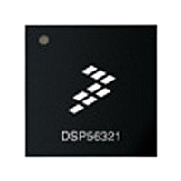
XC56309VL100A Freescale Semiconductor, XC56309VL100A Datasheet - Page 71

XC56309VL100A
Manufacturer Part Number
XC56309VL100A
Description
IC DSP 24BIT 100MHZ 196-MAPBGA
Manufacturer
Freescale Semiconductor
Series
DSP563xxr
Type
Fixed Pointr
Specifications of XC56309VL100A
Interface
Host Interface, SSI, SCI
Clock Rate
100MHz
Non-volatile Memory
ROM (576 B)
On-chip Ram
24kB
Voltage - I/o
3.30V
Voltage - Core
3.30V
Operating Temperature
-40°C ~ 100°C
Mounting Type
Surface Mount
Package / Case
196-MAPBGA
Device Core Size
24b
Format
Fixed Point
Clock Freq (max)
100MHz
Mips
100
Device Input Clock Speed
100MHz
Ram Size
102KB
Operating Supply Voltage (typ)
3.3V
Operating Supply Voltage (min)
3V
Operating Supply Voltage (max)
3.6V
Operating Temp Range
-40C to 100C
Operating Temperature Classification
Industrial
Mounting
Surface Mount
Pin Count
196
Package Type
MA-BGA
Lead Free Status / RoHS Status
Lead free / RoHS Compliant
Available stocks
Company
Part Number
Manufacturer
Quantity
Price
Company:
Part Number:
XC56309VL100A
Manufacturer:
Freescale Semiconductor
Quantity:
10 000
Company:
Part Number:
XC56309VL100AR2
Manufacturer:
Freescale Semiconductor
Quantity:
10 000
- Current page: 71 of 284
- Download datasheet (4Mb)
Freescale Semiconductor
Bit Number
17
16
15
14
13
12
11
Table 4-3. Operating Mode Register (OMR) Bit Definitions (Continued)
Bit Name
EUN
APD
XYS
ATE
ABE
BRT
TAS
Reset Value
0
0
0
0
0
0
0
DSP56309 User’s Manual, Rev. 1
Stack Extension Underflow Flag
Set when a stack underflow occurs in Extended Stack mode. Extended stack
underflow is recognized when a pull operation is requested, SP = 0, and the
SEN bit enables Extended mode. The EUN flag is a sticky bit (that is, cleared
only by hardware reset or by an explicit MOVEC operation to the OMR).
Transition of the EUN flag from zero to one causes a Priority Level 3
(Non-maskable) stack error exception.
NOTE: While the chip is in Extended Stack mode, the UF bit in the SP acts
like a normal counter bit.
Stack Extension XY Select
Determines whether the stack extension is mapped onto X or Y memory
space. If the bit is clear, then the stack extension is mapped onto the X
memory space. If the XYS bit is set, the stack extension is mapped to the Y
memory space.
Address Trace Enable
When set, the Address Trace Enable (ATE) bit enables Address Trace
mode. The Address Trace mode is a debugging tool that reflects internal
memory accesses at the external bus address.
Address Attribute Priority Disable
Disables the priority assigned to the Address Attribute signals (AA[0–3]).
When APD = 0 (default setting), the four Address Attribute signals each have
a certain priority: AA3 has the highest priority, AA0 has the lowest priority.
Therefore, only one AA signal can be active at one time. This allows
continuous partitioning of external memory; however, certain functions, such
as using the AA signals as additional address lines, require the use of
additional interface hardware. When APD is set, the priority mechanism is
disabled, allowing more than one AA signal to be active simultaneously.
Therefore, the AA signals can be used as additional address lines without
the need for additional interface hardware. For details on the Address
Attribute Registers, see Section 4.6.3, Address Attribute Registers
(AAR[0–3]) , on page 4-26.
Asynchronous Bus Arbitration Enable
Eliminates the setup and hold time requirements for BB and BG, and
substitutes a required non-overlap interval between the deassertion of one
BG input to a DSP56300 family device and the assertion of a second BG
input to a second DSP56300 family device on the same bus. When the ABE
bit is set, the BG and BB inputs are synchronized. This synchronization
causes a delay between a change in BG or BB until this change is actually
accepted by the receiving device.
Bus Release Timing
Selects between fast or slow bus release. If BRT is cleared, a Fast Bus
Release mode is selected (that is, no additional cycles are added to the
access and BB is not guaranteed to be the last Port A pin that is tri-stated at
the end of the access). If BRT is set, a Slow Bus Release mode is selected
(that is, an additional cycle is added to the access, and BB is the last Port A
pin that is tri-stated at the end of the access).
TA Synchronize Select
Selects the synchronization method for the input Port A pin—TA (Transfer
Acknowledge). If TAS is cleared, you are responsible for asserting the TA
pin in synchrony with the chip clock, as described in the technical data sheet.
If TAS is set, the TA input pin is synchronized inside the chip, thus
eliminating the need for an off-chip synchronizer. Note that the TAS bit has
no effect when the TA pin is deasserted: you are responsible for deasserting
the TA pin in synchrony with the chip clock, regardless of the value of TAS.
Description
Central Processor Unit (CPU) Registers
4-13
Related parts for XC56309VL100A
Image
Part Number
Description
Manufacturer
Datasheet
Request
R
Part Number:
Description:
Manufacturer:
Freescale Semiconductor, Inc
Datasheet:
Part Number:
Description:
Manufacturer:
Freescale Semiconductor, Inc
Datasheet:
Part Number:
Description:
Manufacturer:
Freescale Semiconductor, Inc
Datasheet:
Part Number:
Description:
Manufacturer:
Freescale Semiconductor, Inc
Datasheet:
Part Number:
Description:
Manufacturer:
Freescale Semiconductor, Inc
Datasheet:
Part Number:
Description:
Manufacturer:
Freescale Semiconductor, Inc
Datasheet:
Part Number:
Description:
Manufacturer:
Freescale Semiconductor, Inc
Datasheet:
Part Number:
Description:
Manufacturer:
Freescale Semiconductor, Inc
Datasheet:
Part Number:
Description:
Manufacturer:
Freescale Semiconductor, Inc
Datasheet:
Part Number:
Description:
Manufacturer:
Freescale Semiconductor, Inc
Datasheet:
Part Number:
Description:
Manufacturer:
Freescale Semiconductor, Inc
Datasheet:
Part Number:
Description:
Manufacturer:
Freescale Semiconductor, Inc
Datasheet:
Part Number:
Description:
Manufacturer:
Freescale Semiconductor, Inc
Datasheet:
Part Number:
Description:
Manufacturer:
Freescale Semiconductor, Inc
Datasheet:
Part Number:
Description:
Manufacturer:
Freescale Semiconductor, Inc
Datasheet:


