MC9S12XA256CAL Freescale Semiconductor, MC9S12XA256CAL Datasheet - Page 178
MC9S12XA256CAL
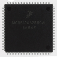
Manufacturer Part Number
MC9S12XA256CAL
Description
IC MCU 256K FLASH 112-LQFP
Manufacturer
Freescale Semiconductor
Series
HCS12r
Specifications of MC9S12XA256CAL
Core Processor
HCS12X
Core Size
16-Bit
Speed
80MHz
Connectivity
EBI/EMI, I²C, IrDA, LIN, SCI, SPI
Peripherals
LVD, POR, PWM, WDT
Number Of I /o
91
Program Memory Size
256KB (256K x 8)
Program Memory Type
FLASH
Eeprom Size
4K x 8
Ram Size
16K x 8
Voltage - Supply (vcc/vdd)
2.35 V ~ 5.5 V
Data Converters
A/D 16x10b
Oscillator Type
External
Operating Temperature
-40°C ~ 85°C
Package / Case
112-LQFP
No. Of I/o's
91
Eeprom Memory Size
4KB
Ram Memory Size
16KB
Cpu Speed
80MHz
No. Of Timers
1
No. Of Pwm Channels
8
Digital Ic Case Style
LQFP
Rohs Compliant
Yes
Processor Series
S12XA
Core
HCS12
Data Bus Width
16 bit
Data Ram Size
16 KB
Interface Type
CAN, I2C, SCI, SPI
Maximum Clock Frequency
40 MHz
Number Of Programmable I/os
91
Number Of Timers
12
Maximum Operating Temperature
+ 85 C
Mounting Style
SMD/SMT
3rd Party Development Tools
EWHCS12
Development Tools By Supplier
EVB9S12XDP512E
Minimum Operating Temperature
- 40 C
On-chip Adc
2 (10 bit, 16 Channel)
Package
112LQFP
Family Name
HCS12
Maximum Speed
40 MHz
Operating Supply Voltage
2.5|5 V
Lead Free Status / RoHS Status
Lead free / RoHS Compliant
Available stocks
Company
Part Number
Manufacturer
Quantity
Price
Company:

Part Number:
MC9S12XA256CAL
Manufacturer:
AD
Quantity:
101
Company:
Part Number:
MC9S12XA256CAL
Manufacturer:
Freescale Semiconductor
Quantity:
10 000
Part Number:
MC9S12XA256CAL
Manufacturer:
FREESCALE
Quantity:
20 000


Chapter 5 Analog-to-Digital Converter (S12ATD10B8CV2)
5.3.2.11
Read: Anytime
Write: Anytime
5.3.2.12
The data port associated with the ATD can be configured as general-purpose I/O or input only, as specified
in the device overview. The port pins are shared with the analog A/D inputs AN7–0.
Read: Anytime
Write: Anytime, no effect
The A/D input channels may be used for general purpose digital input.
178
Function
PTAD[7:0]
IEN[7:0]
Reset
Reset
Field
Field
7–0
7–0
Pin
W
W
R
R
PTAD7
IEN7
AN7
ATD Digital Input Enable on channel x (x = 7, 6, 5, 4, 3, 2, 1, 0) — This bit controls the digital input buffer from
the analog input pin (ANx) to PTADx data register.
0 Disable digital input buffer to PTADx
1 Enable digital input buffer to PTADx.
Note: Setting this bit will enable the corresponding digital input buffer continuously. If this bit is set while
A/D Channel x (ANx) Digital Input (x = 7, 6, 5, 4, 3, 2, 1, 0) — If the digital input buffer on the ANx pin is enabled
(IENx = 1) or channel x is enabled as external trigger (ETRIGE = 1,ETRIGCH[2–0] = x,ETRIGSEL = 0) read
returns the logic level on ANx pin (signal potentials not meeting V
indeterminate value).
If the digital input buffers are disabled (IENx = 0) and channel x is not enabled as external trigger, read returns
a “1”.
Reset sets all PORTAD0 bits to “1”.
ATD Input Enable Register (ATDDIEN)
Port Data Register (PORTAD)
0
1
7
7
simultaneously using it as an analog port, there is potentially increased power consumption because the
digital input buffer maybe in the linear region.
= Unimplemented or Reserved
PTAD6
IEN6
AN6
0
1
6
6
Figure 5-13. ATD Input Enable Register (ATDDIEN)
Figure 5-14. Port Data Register (PORTAD)
Table 5-21. ATDDIEN Field Descriptions
Table 5-22. PORTAD Field Descriptions
PTAD5
MC9S12XDP512 Data Sheet, Rev. 2.21
IEN5
AN5
0
1
5
5
PTAD4
IEN4
AN4
0
1
4
4
Description
Description
PTAD3
IEN3
AN3
0
1
3
3
IL
or V
PTAD2
IH
IEN2
AN2
0
1
specifications will have an
2
2
Freescale Semiconductor
PTAD1
IEN1
AN1
0
1
1
1
PTAD0
IEN0
AN0
0
1
0
0
Related parts for MC9S12XA256CAL
Image
Part Number
Description
Manufacturer
Datasheet
Request
R

Part Number:
Description:
Manufacturer:
Freescale Semiconductor, Inc
Datasheet:
Part Number:
Description:
Manufacturer:
Freescale Semiconductor, Inc
Datasheet:
Part Number:
Description:
Manufacturer:
Freescale Semiconductor, Inc
Datasheet:
Part Number:
Description:
Manufacturer:
Freescale Semiconductor, Inc
Datasheet:
Part Number:
Description:
Manufacturer:
Freescale Semiconductor, Inc
Datasheet:
Part Number:
Description:
Manufacturer:
Freescale Semiconductor, Inc
Datasheet:
Part Number:
Description:
Manufacturer:
Freescale Semiconductor, Inc
Datasheet:
Part Number:
Description:
Manufacturer:
Freescale Semiconductor, Inc
Datasheet:
Part Number:
Description:
Manufacturer:
Freescale Semiconductor, Inc
Datasheet:
Part Number:
Description:
Manufacturer:
Freescale Semiconductor, Inc
Datasheet:
Part Number:
Description:
Manufacturer:
Freescale Semiconductor, Inc
Datasheet:
Part Number:
Description:
Manufacturer:
Freescale Semiconductor, Inc
Datasheet:
Part Number:
Description:
Manufacturer:
Freescale Semiconductor, Inc
Datasheet:
Part Number:
Description:
Manufacturer:
Freescale Semiconductor, Inc
Datasheet:
Part Number:
Description:
Manufacturer:
Freescale Semiconductor, Inc
Datasheet: