MC9S12XA256CAL Freescale Semiconductor, MC9S12XA256CAL Datasheet - Page 1154
MC9S12XA256CAL
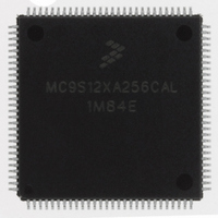
Manufacturer Part Number
MC9S12XA256CAL
Description
IC MCU 256K FLASH 112-LQFP
Manufacturer
Freescale Semiconductor
Series
HCS12r
Specifications of MC9S12XA256CAL
Core Processor
HCS12X
Core Size
16-Bit
Speed
80MHz
Connectivity
EBI/EMI, I²C, IrDA, LIN, SCI, SPI
Peripherals
LVD, POR, PWM, WDT
Number Of I /o
91
Program Memory Size
256KB (256K x 8)
Program Memory Type
FLASH
Eeprom Size
4K x 8
Ram Size
16K x 8
Voltage - Supply (vcc/vdd)
2.35 V ~ 5.5 V
Data Converters
A/D 16x10b
Oscillator Type
External
Operating Temperature
-40°C ~ 85°C
Package / Case
112-LQFP
No. Of I/o's
91
Eeprom Memory Size
4KB
Ram Memory Size
16KB
Cpu Speed
80MHz
No. Of Timers
1
No. Of Pwm Channels
8
Digital Ic Case Style
LQFP
Rohs Compliant
Yes
Processor Series
S12XA
Core
HCS12
Data Bus Width
16 bit
Data Ram Size
16 KB
Interface Type
CAN, I2C, SCI, SPI
Maximum Clock Frequency
40 MHz
Number Of Programmable I/os
91
Number Of Timers
12
Maximum Operating Temperature
+ 85 C
Mounting Style
SMD/SMT
3rd Party Development Tools
EWHCS12
Development Tools By Supplier
EVB9S12XDP512E
Minimum Operating Temperature
- 40 C
On-chip Adc
2 (10 bit, 16 Channel)
Package
112LQFP
Family Name
HCS12
Maximum Speed
40 MHz
Operating Supply Voltage
2.5|5 V
Lead Free Status / RoHS Status
Lead free / RoHS Compliant
Available stocks
Company
Part Number
Manufacturer
Quantity
Price
Company:

Part Number:
MC9S12XA256CAL
Manufacturer:
AD
Quantity:
101
Company:
Part Number:
MC9S12XA256CAL
Manufacturer:
Freescale Semiconductor
Quantity:
10 000
Part Number:
MC9S12XA256CAL
Manufacturer:
FREESCALE
Quantity:
20 000


Chapter 28 256 Kbyte Flash Module (S12XFTX256K2V1)
MRDS bits are readable and writable while all remaining bits read 0 and are not writable in normal mode.
The WRALL bit is writable only in special mode to simplify mass erase and erase verify operations. When
writing to the FTSTMOD register in special mode, all unimplemented/reserved bits must be written to 0.
28.3.2.4
The FCNFG register enables the Flash interrupts and gates the security backdoor writes.
1156
MRDS[1:0]
WRALL
Reset
Reset
Field
6:5
4
W
W
R
R
Margin Read Setting — The MRDS[1:0] bits are used to set the sense-amp margin level for reads of the Flash
array as shown in
Write to all Register Banks — If the WRALL bit is set, all banked FDATA registers sharing the same register
address will be written simultaneously during a register write.
0 Write only to the FDATA register bank selected using BKSEL.
1 Write to all FDATA register banks.
Flash Configuration Register (FCNFG)
0
0
0
0
7
7
Figure 28-7. Flash Test Mode Register (FTSTMOD — Special Mode)
Figure 28-6. Flash Test Mode Register (FTSTMOD —Normal Mode)
= Unimplemented or Reserved
= Unimplemented or Reserved
0
0
6
6
1 Flash array reads will be sensitive to program margin.
2 Flash array reads will be sensitive to erase margin.
Table
MRDS
MRDS
MRDS[1:0]
Table 28-7. FTSTMOD Margin Read Settings
Table 28-6. FTSTMOD Field Descriptions
28-7.
00
01
10
11
MC9S12XDP512 Data Sheet, Rev. 2.21
0
0
5
5
WRALL
0
0
0
4
4
Margin Read Setting
Description
Program Margin
Erase Margin
Normal
Normal
0
0
0
0
3
3
2
1
0
0
0
0
2
2
Freescale Semiconductor
0
0
0
0
1
1
0
0
0
0
0
0
Related parts for MC9S12XA256CAL
Image
Part Number
Description
Manufacturer
Datasheet
Request
R

Part Number:
Description:
Manufacturer:
Freescale Semiconductor, Inc
Datasheet:
Part Number:
Description:
Manufacturer:
Freescale Semiconductor, Inc
Datasheet:
Part Number:
Description:
Manufacturer:
Freescale Semiconductor, Inc
Datasheet:
Part Number:
Description:
Manufacturer:
Freescale Semiconductor, Inc
Datasheet:
Part Number:
Description:
Manufacturer:
Freescale Semiconductor, Inc
Datasheet:
Part Number:
Description:
Manufacturer:
Freescale Semiconductor, Inc
Datasheet:
Part Number:
Description:
Manufacturer:
Freescale Semiconductor, Inc
Datasheet:
Part Number:
Description:
Manufacturer:
Freescale Semiconductor, Inc
Datasheet:
Part Number:
Description:
Manufacturer:
Freescale Semiconductor, Inc
Datasheet:
Part Number:
Description:
Manufacturer:
Freescale Semiconductor, Inc
Datasheet:
Part Number:
Description:
Manufacturer:
Freescale Semiconductor, Inc
Datasheet:
Part Number:
Description:
Manufacturer:
Freescale Semiconductor, Inc
Datasheet:
Part Number:
Description:
Manufacturer:
Freescale Semiconductor, Inc
Datasheet:
Part Number:
Description:
Manufacturer:
Freescale Semiconductor, Inc
Datasheet:
Part Number:
Description:
Manufacturer:
Freescale Semiconductor, Inc
Datasheet: