P89V662FBC,557 NXP Semiconductors, P89V662FBC,557 Datasheet - Page 89
P89V662FBC,557
Manufacturer Part Number
P89V662FBC,557
Description
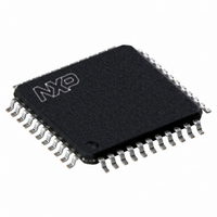
IC 80C51 MCU FLASH 32K 44-TQFP
Manufacturer
NXP Semiconductors
Series
89Vr
Datasheet
1.P89V660FBC557.pdf
(89 pages)
Specifications of P89V662FBC,557
Program Memory Type
FLASH
Program Memory Size
32KB (32K x 8)
Package / Case
44-TQFP
Core Processor
8051
Core Size
8-Bit
Speed
40MHz
Connectivity
I²C, SPI, UART/USART
Peripherals
POR, PWM, WDT
Number Of I /o
36
Ram Size
1K x 8
Voltage - Supply (vcc/vdd)
4.5 V ~ 5.5 V
Oscillator Type
Internal
Operating Temperature
-40°C ~ 85°C
Processor Series
P89V6x
Core
80C51
Data Bus Width
8 bit
Data Ram Size
1 KB
Interface Type
I2C/UART
Maximum Clock Frequency
40 MHz
Number Of Programmable I/os
36
Number Of Timers
3
Operating Supply Voltage
4.5 V to 5.5 V
Maximum Operating Temperature
+ 85 C
Mounting Style
SMD/SMT
3rd Party Development Tools
PK51, CA51, A51, ULINK2
Minimum Operating Temperature
- 40 C
Lead Free Status / RoHS Status
Lead free / RoHS Compliant
For Use With
622-1001 - USB IN-CIRCUIT PROG 80C51ISP
Eeprom Size
-
Data Converters
-
Lead Free Status / Rohs Status
Lead free / RoHS Compliant
Other names
568-2435
935280832557
P89V662FBC
935280832557
P89V662FBC
Available stocks
Company
Part Number
Manufacturer
Quantity
Price
Company:

Part Number:
P89V662FBC,557
Manufacturer:
Maxim
Quantity:
260
Company:
Part Number:
P89V662FBC,557
Manufacturer:
NXP Semiconductors
Quantity:
10 000


NXP Semiconductors
15. Contents
1
2
2.1
2.2
2.3
3
3.1
4
5
5.1
5.2
6
6.1
6.2
6.2.1
6.2.2
6.2.3
6.3
6.3.1
6.3.2
6.3.3
6.3.4
6.3.5
6.3.6
6.3.7
6.3.8
6.4
6.4.1
6.4.2
6.4.3
6.4.4
6.4.5
6.4.5.1
6.4.5.2
6.4.5.3
6.4.5.4
6.5
6.5.1
6.5.2
6.5.3
6.5.4
6.6
6.6.1
6.6.2
6.6.3
6.6.4
6.6.5
General description . . . . . . . . . . . . . . . . . . . . . . 1
Features . . . . . . . . . . . . . . . . . . . . . . . . . . . . . . . 1
Ordering information . . . . . . . . . . . . . . . . . . . . . 2
Block diagram . . . . . . . . . . . . . . . . . . . . . . . . . . 3
Pinning information . . . . . . . . . . . . . . . . . . . . . . 4
Functional description . . . . . . . . . . . . . . . . . . 10
Principal features . . . . . . . . . . . . . . . . . . . . . . . 1
Additional features . . . . . . . . . . . . . . . . . . . . . . 1
Comparison to the P89C660/662/664 devices . 2
Ordering options . . . . . . . . . . . . . . . . . . . . . . . . 3
Pinning . . . . . . . . . . . . . . . . . . . . . . . . . . . . . . . 4
Pin description . . . . . . . . . . . . . . . . . . . . . . . . . 6
Special function registers . . . . . . . . . . . . . . . . 10
Memory organization . . . . . . . . . . . . . . . . . . . 14
Expanded data RAM addressing . . . . . . . . . . 14
Dual data pointers. . . . . . . . . . . . . . . . . . . . . . 16
Reset . . . . . . . . . . . . . . . . . . . . . . . . . . . . . . . 17
Flash memory. . . . . . . . . . . . . . . . . . . . . . . . . 18
Flash organization . . . . . . . . . . . . . . . . . . . . . 18
Features . . . . . . . . . . . . . . . . . . . . . . . . . . . . . 18
Boot block . . . . . . . . . . . . . . . . . . . . . . . . . . . . 19
Power-on reset code execution. . . . . . . . . . . . 19
Hardware activation of the bootloader . . . . . . 19
ISP . . . . . . . . . . . . . . . . . . . . . . . . . . . . . . . . . 19
Using ISP . . . . . . . . . . . . . . . . . . . . . . . . . . . . 19
IAP method . . . . . . . . . . . . . . . . . . . . . . . . . . . 23
I
I
I
I
I
I
Master transmitter mode. . . . . . . . . . . . . . . . . 28
Master receiver mode . . . . . . . . . . . . . . . . . . . 29
Slave receiver mode . . . . . . . . . . . . . . . . . . . . 30
Slave transmitter mode . . . . . . . . . . . . . . . . . . 30
Timers/counters 0 and 1 . . . . . . . . . . . . . . . . . 38
Mode 0 . . . . . . . . . . . . . . . . . . . . . . . . . . . . . . 40
Mode 1 . . . . . . . . . . . . . . . . . . . . . . . . . . . . . . 41
Mode 2 . . . . . . . . . . . . . . . . . . . . . . . . . . . . . . 41
Mode 3 . . . . . . . . . . . . . . . . . . . . . . . . . . . . . . 42
Timer 2 . . . . . . . . . . . . . . . . . . . . . . . . . . . . . . 42
Capture mode . . . . . . . . . . . . . . . . . . . . . . . . . 44
Auto-reload mode (up or down-counter) . . . . . 45
Programmable clock-out . . . . . . . . . . . . . . . . . 46
Baud rate generator mode . . . . . . . . . . . . . . . 47
Summary of baud rate equations . . . . . . . . . . 48
2
2
2
2
2
2
C-bus interface . . . . . . . . . . . . . . . . . . . . . . . 24
C-bus data register. . . . . . . . . . . . . . . . . . . . 26
C-bus slave address register . . . . . . . . . . . . 26
C-bus control register . . . . . . . . . . . . . . . . . . 26
C-bus status register . . . . . . . . . . . . . . . . . . 28
C-bus operation modes . . . . . . . . . . . . . . . . 28
80C51 with 512 B/1 kB/2 kB RAM, dual I
6.7
6.7.1
6.7.2
6.7.3
6.7.4
6.7.5
6.7.6
6.7.7
6.7.8
6.7.9
6.8
6.8.1
6.8.2
6.9
6.10
6.10.1
6.10.2
6.10.3
6.10.4
6.10.5
6.11
6.12
6.13
6.13.1
6.13.2
6.14
6.14.1
6.14.2
7
8
9
9.1
10
11
12
13
13.1
13.2
13.3
13.4
14
15
Please be aware that important notices concerning this document and the product(s)
described herein, have been included in section ‘Legal information’.
© NXP B.V. 2008.
For more information, please visit: http://www.nxp.com
For sales office addresses, please send an email to: salesaddresses@nxp.com
Limiting values . . . . . . . . . . . . . . . . . . . . . . . . 71
Static characteristics . . . . . . . . . . . . . . . . . . . 71
Dynamic characteristics . . . . . . . . . . . . . . . . . 74
Package outline . . . . . . . . . . . . . . . . . . . . . . . . 84
Abbreviations . . . . . . . . . . . . . . . . . . . . . . . . . 86
Revision history . . . . . . . . . . . . . . . . . . . . . . . 87
Legal information . . . . . . . . . . . . . . . . . . . . . . 88
Contact information . . . . . . . . . . . . . . . . . . . . 88
Contents. . . . . . . . . . . . . . . . . . . . . . . . . . . . . . 89
UARTs . . . . . . . . . . . . . . . . . . . . . . . . . . . . . . 48
Mode 0 . . . . . . . . . . . . . . . . . . . . . . . . . . . . . . 49
Mode 1 . . . . . . . . . . . . . . . . . . . . . . . . . . . . . . 49
Mode 2 . . . . . . . . . . . . . . . . . . . . . . . . . . . . . . 49
Mode 3 . . . . . . . . . . . . . . . . . . . . . . . . . . . . . . 49
Framing error . . . . . . . . . . . . . . . . . . . . . . . . . 50
More about UART mode 1 . . . . . . . . . . . . . . . 50
More about UART modes 2 and 3 . . . . . . . . . 50
Multiprocessor communications . . . . . . . . . . . 51
Automatic address recognition . . . . . . . . . . . . 51
Serial Peripheral Interface (SPI). . . . . . . . . . . 53
SPI features . . . . . . . . . . . . . . . . . . . . . . . . . . 53
SPI description . . . . . . . . . . . . . . . . . . . . . . . . 53
Watchdog timer . . . . . . . . . . . . . . . . . . . . . . . 56
PCA . . . . . . . . . . . . . . . . . . . . . . . . . . . . . . . . 56
PCA capture mode. . . . . . . . . . . . . . . . . . . . . 60
16-bit software timer mode. . . . . . . . . . . . . . . 61
High-speed output mode . . . . . . . . . . . . . . . . 62
Pulse width modulator mode . . . . . . . . . . . . . 63
PCA watchdog timer . . . . . . . . . . . . . . . . . . . 64
Security bits . . . . . . . . . . . . . . . . . . . . . . . . . . 65
Interrupt priority and polling sequence . . . . . . 65
Power-saving modes . . . . . . . . . . . . . . . . . . . 68
Idle mode . . . . . . . . . . . . . . . . . . . . . . . . . . . . 69
Power-down mode . . . . . . . . . . . . . . . . . . . . . 69
System clock and clock options . . . . . . . . . . . 70
Clock input options and recommended capacitor
values for the oscillator. . . . . . . . . . . . . . . . . . 70
Clock doubling option . . . . . . . . . . . . . . . . . . . 70
Explanation of symbols . . . . . . . . . . . . . . . . . 75
Data sheet status . . . . . . . . . . . . . . . . . . . . . . 88
Definitions . . . . . . . . . . . . . . . . . . . . . . . . . . . 88
Disclaimers. . . . . . . . . . . . . . . . . . . . . . . . . . . 88
Trademarks . . . . . . . . . . . . . . . . . . . . . . . . . . 88
P89V660/662/664
Document identifier: P89V660_662_664_3
Date of release: 10 November 2008
All rights reserved.
2
C-bus, SPI
Related parts for P89V662FBC,557
Image
Part Number
Description
Manufacturer
Datasheet
Request
R

Part Number:
Description:
NXP Semiconductors designed the LPC2420/2460 microcontroller around a 16-bit/32-bitARM7TDMI-S CPU core with real-time debug interfaces that include both JTAG andembedded trace
Manufacturer:
NXP Semiconductors
Datasheet:

Part Number:
Description:
NXP Semiconductors designed the LPC2458 microcontroller around a 16-bit/32-bitARM7TDMI-S CPU core with real-time debug interfaces that include both JTAG andembedded trace
Manufacturer:
NXP Semiconductors
Datasheet:
Part Number:
Description:
NXP Semiconductors designed the LPC2468 microcontroller around a 16-bit/32-bitARM7TDMI-S CPU core with real-time debug interfaces that include both JTAG andembedded trace
Manufacturer:
NXP Semiconductors
Datasheet:
Part Number:
Description:
NXP Semiconductors designed the LPC2470 microcontroller, powered by theARM7TDMI-S core, to be a highly integrated microcontroller for a wide range ofapplications that require advanced communications and high quality graphic displays
Manufacturer:
NXP Semiconductors
Datasheet:
Part Number:
Description:
NXP Semiconductors designed the LPC2478 microcontroller, powered by theARM7TDMI-S core, to be a highly integrated microcontroller for a wide range ofapplications that require advanced communications and high quality graphic displays
Manufacturer:
NXP Semiconductors
Datasheet:
Part Number:
Description:
The Philips Semiconductors XA (eXtended Architecture) family of 16-bit single-chip microcontrollers is powerful enough to easily handle the requirements of high performance embedded applications, yet inexpensive enough to compete in the market for hi
Manufacturer:
NXP Semiconductors
Datasheet:
Part Number:
Description:
The XA-S3 device is a member of Philips Semiconductors? XA(eXtended Architecture) family of high performance 16-bitsingle-chip microcontrollers
Manufacturer:
NXP Semiconductors
Datasheet:

Part Number:
Description:
The NXP BlueStreak LH75401/LH75411 family consists of two low-cost 16/32-bit System-on-Chip (SoC) devices
Manufacturer:
NXP Semiconductors
Datasheet:
Part Number:
Description:
The NXP LPC3130/3131 combine an 180 MHz ARM926EJ-S CPU core, high-speed USB2
Manufacturer:
NXP Semiconductors
Datasheet:
Part Number:
Description:
The NXP LPC3141 combine a 270 MHz ARM926EJ-S CPU core, High-speed USB 2
Manufacturer:
NXP Semiconductors
Part Number:
Description:
The NXP LPC3143 combine a 270 MHz ARM926EJ-S CPU core, High-speed USB 2
Manufacturer:
NXP Semiconductors

Part Number:
Description:
The NXP LPC3152 combines an 180 MHz ARM926EJ-S CPU core, High-speed USB 2
Manufacturer:
NXP Semiconductors
Part Number:
Description:
The NXP LPC3154 combines an 180 MHz ARM926EJ-S CPU core, High-speed USB 2
Manufacturer:
NXP Semiconductors

Part Number:
Description:
Standard level N-channel enhancement mode Field-Effect Transistor (FET) in a plastic package using NXP High-Performance Automotive (HPA) TrenchMOS technology
Manufacturer:
NXP Semiconductors
Datasheet: