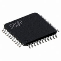
P89V662FBC,557 NXP Semiconductors, P89V662FBC,557 Datasheet - Page 53

P89V662FBC,557
Manufacturer Part Number
P89V662FBC,557
Description
IC 80C51 MCU FLASH 32K 44-TQFP
Manufacturer
NXP Semiconductors
Series
89Vr
Datasheet
1.P89V660FBC557.pdf
(89 pages)
Specifications of P89V662FBC,557
Program Memory Type
FLASH
Program Memory Size
32KB (32K x 8)
Package / Case
44-TQFP
Core Processor
8051
Core Size
8-Bit
Speed
40MHz
Connectivity
I²C, SPI, UART/USART
Peripherals
POR, PWM, WDT
Number Of I /o
36
Ram Size
1K x 8
Voltage - Supply (vcc/vdd)
4.5 V ~ 5.5 V
Oscillator Type
Internal
Operating Temperature
-40°C ~ 85°C
Processor Series
P89V6x
Core
80C51
Data Bus Width
8 bit
Data Ram Size
1 KB
Interface Type
I2C/UART
Maximum Clock Frequency
40 MHz
Number Of Programmable I/os
36
Number Of Timers
3
Operating Supply Voltage
4.5 V to 5.5 V
Maximum Operating Temperature
+ 85 C
Mounting Style
SMD/SMT
3rd Party Development Tools
PK51, CA51, A51, ULINK2
Minimum Operating Temperature
- 40 C
Lead Free Status / RoHS Status
Lead free / RoHS Compliant
For Use With
622-1001 - USB IN-CIRCUIT PROG 80C51ISP
Eeprom Size
-
Data Converters
-
Lead Free Status / Rohs Status
Lead free / RoHS Compliant
Other names
568-2435
935280832557
P89V662FBC
935280832557
P89V662FBC
Available stocks
Company
Part Number
Manufacturer
Quantity
Price
Company:
Part Number:
P89V662FBC,557
Manufacturer:
Maxim
Quantity:
260
Company:
Part Number:
P89V662FBC,557
Manufacturer:
NXP Semiconductors
Quantity:
10 000
NXP Semiconductors
P89V660_662_664_3
Product data sheet
6.8.1 SPI features
6.8.2 SPI description
6.8 Serial Peripheral Interface (SPI)
In a more complex system the following could be used to select slaves 1 and 2 while
excluding slave 0:
Example 1, slave 0:
SADDR = 1100 0000
--------------------------------------------------- -
Example 2, slave 1:
SADDR = 1110 0000
--------------------------------------------------- -
Example 2, slave 2:
SADDR = 1100 0000
--------------------------------------------------- -
In the above example the differentiation among the 3 slaves is in the lower 3 address bits.
Slave 0 requires that bit 0 = 0 and it can be uniquely addressed by 1110 0110. Slave 1
requires that bit 1 = 0 and it can be uniquely addressed by 1110 0101. Slave 2 requires
that bit 2 = 0 and its unique address is 1110 0011. To select Slaves 0 and 1 and exclude
Slave 2 use address 1110 0100, since it is necessary to make bit 2 = 1 to exclude slave 2.
The Broadcast Address for each slave is created by taking the logical OR of SADDR and
SADEN. Zeros in this result are treated as don’t-cares. In most cases, interpreting the
don’t-cares as ones, the broadcast address will be FF hexadecimal. Upon reset SADDR
and SADEN are loaded with 0s. This produces a given address of all ‘don’t cares’ as well
as a Broadcast address of all ‘don’t cares'. This effectively disables the Automatic
Addressing mode and allows the microcontroller to use standard UART drivers which do
not make use of this feature.
The serial peripheral interface allows high-speed synchronous data transfer between the
P89V660/662/664 and peripheral devices or between several P89V660/662/664 devices.
Figure 23
SADEN = 1111 1001
SADEN = 1111 1010
SADEN = 1111 1100
•
•
•
•
•
•
•
Given = 1100 0XX0
Given = 1110 0X0X
Given = 1100 00XX
Master or slave operation
10 MHz bit frequency (max)
LSB first or MSB first data transfer
Four programmable bit rates
End of transmission (SPIF)
Write collision flag protection (WCOL)
Wake-up from Idle mode (slave mode only)
shows the correspondence between master and slave SPI devices. The SCK
Rev. 03 — 10 November 2008
80C51 with 512 B/1 kB/2 kB RAM, dual I
P89V660/662/664
© NXP B.V. 2008. All rights reserved.
2
C-bus, SPI
53 of 89
(6)
(7)
(8)


