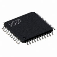
P89V662FBC,557 NXP Semiconductors, P89V662FBC,557 Datasheet - Page 26

P89V662FBC,557
Manufacturer Part Number
P89V662FBC,557
Description
IC 80C51 MCU FLASH 32K 44-TQFP
Manufacturer
NXP Semiconductors
Series
89Vr
Datasheet
1.P89V660FBC557.pdf
(89 pages)
Specifications of P89V662FBC,557
Program Memory Type
FLASH
Program Memory Size
32KB (32K x 8)
Package / Case
44-TQFP
Core Processor
8051
Core Size
8-Bit
Speed
40MHz
Connectivity
I²C, SPI, UART/USART
Peripherals
POR, PWM, WDT
Number Of I /o
36
Ram Size
1K x 8
Voltage - Supply (vcc/vdd)
4.5 V ~ 5.5 V
Oscillator Type
Internal
Operating Temperature
-40°C ~ 85°C
Processor Series
P89V6x
Core
80C51
Data Bus Width
8 bit
Data Ram Size
1 KB
Interface Type
I2C/UART
Maximum Clock Frequency
40 MHz
Number Of Programmable I/os
36
Number Of Timers
3
Operating Supply Voltage
4.5 V to 5.5 V
Maximum Operating Temperature
+ 85 C
Mounting Style
SMD/SMT
3rd Party Development Tools
PK51, CA51, A51, ULINK2
Minimum Operating Temperature
- 40 C
Lead Free Status / RoHS Status
Lead free / RoHS Compliant
For Use With
622-1001 - USB IN-CIRCUIT PROG 80C51ISP
Eeprom Size
-
Data Converters
-
Lead Free Status / Rohs Status
Lead free / RoHS Compliant
Other names
568-2435
935280832557
P89V662FBC
935280832557
P89V662FBC
Available stocks
Company
Part Number
Manufacturer
Quantity
Price
Company:
Part Number:
P89V662FBC,557
Manufacturer:
Maxim
Quantity:
260
Company:
Part Number:
P89V662FBC,557
Manufacturer:
NXP Semiconductors
Quantity:
10 000
NXP Semiconductors
P89V660_662_664_3
Product data sheet
6.4.1 I
6.4.2 I
6.4.3 I
S1DAT register contains the data to be transmitted or the data received. The CPU can
read and write to this 8-bit register while it is not in the process of shifting a byte. Thus this
register should only be accessed when the SI bit is set. Data in S1DAT remains stable as
long as the SI bit is set. Data in S1DAT is always shifted from right to left: the first bit to be
transmitted is the MSB (bit 7), and after a byte has been received, the first bit of received
data is located at the MSB of S1DAT.
The S1ADR register is readable and writable, and is only used when the I
is set to slave mode. In master mode, this register has no effect. The LSB of S1ADR is
general call bit. When this bit is set, the general call address (00H) is recognized.
Table 13.
Table 14.
The CPU can read and write this register. There are two bits are affected by hardware: the
SI bit and the STO bit. The SI bit is set by hardware and the STO bit is cleared by
hardware.
CR2:0 determines the SCL source and frequency when the I
slave mode these bits are ignored and the bus will automatically synchronize with any
clock frequency up to 100 kHz from the master I
programmed by the user in 8 bit auto-reload mode (Mode 2) when used as the SCL
source. See
The STA bit is START flag. Setting this bit causes the I
mode and attempt transmitting a START condition or transmitting a repeated START
condition when it is already in master mode.
The STO bit is STOP flag. Setting this bit causes the I
condition in master mode, or recovering from an error condition in slave mode.
If the STA and STO are both set, then a STOP condition is transmitted to the I
in master mode, and transmits a START condition afterwards. If it is in slave mode, an
internal STOP condition will be generated, but it is not transmitted to the bus.
Bit
Symbol
Reset
Bit Symbol
7:1 S1ADR7:1 7 bit own slave address. When in master mode, the contents of this register has
0
2
2
2
C-bus data register
C-bus slave address register
C-bus control register
S1GC
7
S1ADR.6 S1ADR.5 S1ADR.4 S1ADR.3 S1ADR.2 S1ADR.1 S1ADR.0 S1GC
0
I
I
2
2
C-bus slave address register (S1ADR - address DBH) bit allocation
C-bus slave address register (S1ADR - address DBH) bit description
Table
Description
no effect.
General call bit. When set, the general call address (00H) is recognized,
otherwise it is ignored.
17.
6
0
Rev. 03 — 10 November 2008
5
0
80C51 with 512 B/1 kB/2 kB RAM, dual I
4
0
2
C-bus device. Timer 1 should be
3
0
P89V660/662/664
2
C-bus interface to transmit a STOP
2
C-bus interface to enter master
2
0
2
C-bus is in master mode. In
1
0
© NXP B.V. 2008. All rights reserved.
2
C-bus interface
2
2
C-bus if it is
C-bus, SPI
0
0
26 of 89


