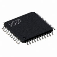
P89V662FBC,557 NXP Semiconductors, P89V662FBC,557 Datasheet - Page 28

P89V662FBC,557
Manufacturer Part Number
P89V662FBC,557
Description
IC 80C51 MCU FLASH 32K 44-TQFP
Manufacturer
NXP Semiconductors
Series
89Vr
Datasheet
1.P89V660FBC557.pdf
(89 pages)
Specifications of P89V662FBC,557
Program Memory Type
FLASH
Program Memory Size
32KB (32K x 8)
Package / Case
44-TQFP
Core Processor
8051
Core Size
8-Bit
Speed
40MHz
Connectivity
I²C, SPI, UART/USART
Peripherals
POR, PWM, WDT
Number Of I /o
36
Ram Size
1K x 8
Voltage - Supply (vcc/vdd)
4.5 V ~ 5.5 V
Oscillator Type
Internal
Operating Temperature
-40°C ~ 85°C
Processor Series
P89V6x
Core
80C51
Data Bus Width
8 bit
Data Ram Size
1 KB
Interface Type
I2C/UART
Maximum Clock Frequency
40 MHz
Number Of Programmable I/os
36
Number Of Timers
3
Operating Supply Voltage
4.5 V to 5.5 V
Maximum Operating Temperature
+ 85 C
Mounting Style
SMD/SMT
3rd Party Development Tools
PK51, CA51, A51, ULINK2
Minimum Operating Temperature
- 40 C
Lead Free Status / RoHS Status
Lead free / RoHS Compliant
For Use With
622-1001 - USB IN-CIRCUIT PROG 80C51ISP
Eeprom Size
-
Data Converters
-
Lead Free Status / Rohs Status
Lead free / RoHS Compliant
Other names
568-2435
935280832557
P89V662FBC
935280832557
P89V662FBC
Available stocks
Company
Part Number
Manufacturer
Quantity
Price
Company:
Part Number:
P89V662FBC,557
Manufacturer:
Maxim
Quantity:
260
Company:
Part Number:
P89V662FBC,557
Manufacturer:
NXP Semiconductors
Quantity:
10 000
NXP Semiconductors
Table 17.
P89V660_662_664_3
Product data sheet
CR2:0
101
110
111
6-clock mode
6 MHz
100
200
0.49 < 62.5
I
2
C-bus clock rates
6.4.5.1 Master transmitter mode
6.4.4 I
6.4.5 I
This is a read-only register. It contains the status code of the I
three bits are always 0. There are 26 possible status codes. When the code is F8H, there
is no relevant information available and SI bit is not set. All other 25 status codes
correspond to defined I
set. Refer to
Table 18.
Table 19.
In this mode data is transmitted from master to slave. Before the Master Transmitter mode
can be entered, S1CON must be initialized as follows:
Table 20.
CR2:0 define the bit rate (See
function. If the AA bit is 0, it will not acknowledge its own slave address or the general call
address in the event of another device becoming master of the bus and it can not enter
slave mode. STA, STO, and SI bits must be cleared to 0.
The first byte transmitted contains the slave address of the receiving device (7 bits) and
the data direction bit. In this case, the data direction bit (R/W) will be logic 0 indicating a
write. Data is transmitted 8 bits at a time. After each byte is transmitted, an acknowledge
bit is received. START and STOP conditions are output to indicate the beginning and the
end of a serial transfer.
Bit
Symbol
Reset
Bit Symbol
7:3 SC[4:0]
2:0 -
Bit
Symbol
Value
2
2
C-bus status register
C-bus operation modes
12 MHZ
200
400
0.98 < 50.0
…continued
7
SC.4
0
7
CR2
bit rate
I
I
I
2
2
2
Bit frequency at f
C-bus status register (S1STA - address D9H) bit allocation
C-bus status register (S1STA - address D9H) bit description
C-bus control register (S1CON - address D8H)
Table 22
Description
I
Reserved, are always set to 0.
2
C-bus Status code.
6
SC.3
0
6
ENS1
1
Rev. 03 — 10 November 2008
12-clock mode
6 MHz
50
100
0.24 < 62.5
to
2
C-bus states. When any of these states entered, the SI bit will be
Table 25
osc
5
SC.2
0
5
STA
0
Table
for details.
80C51 with 512 B/1 kB/2 kB RAM, dual I
17). ENS1 must be set to 1 to enable the I
12 MHz
100
200
0.49 < 62.5
4
SC.1
0
4
STO
0
3
SC.0
0
3
SI
0
P89V660/662/664
f
6X
60
30
48 x (Timer 1
reload)
osc
divided by
2
0
0
2
AA
x
2
C-bus interface. The least
1
0
0
1
CR1
bit rate
© NXP B.V. 2008. All rights reserved.
12X
120
60
96 x (Timer 1
reload)
2
C-bus, SPI
2
C-bus
0
0
0
0
CR0
bit rate
28 of 89


