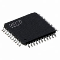
P89V662FBC,557 NXP Semiconductors, P89V662FBC,557 Datasheet - Page 18

P89V662FBC,557
Manufacturer Part Number
P89V662FBC,557
Description
IC 80C51 MCU FLASH 32K 44-TQFP
Manufacturer
NXP Semiconductors
Series
89Vr
Datasheet
1.P89V660FBC557.pdf
(89 pages)
Specifications of P89V662FBC,557
Program Memory Type
FLASH
Program Memory Size
32KB (32K x 8)
Package / Case
44-TQFP
Core Processor
8051
Core Size
8-Bit
Speed
40MHz
Connectivity
I²C, SPI, UART/USART
Peripherals
POR, PWM, WDT
Number Of I /o
36
Ram Size
1K x 8
Voltage - Supply (vcc/vdd)
4.5 V ~ 5.5 V
Oscillator Type
Internal
Operating Temperature
-40°C ~ 85°C
Processor Series
P89V6x
Core
80C51
Data Bus Width
8 bit
Data Ram Size
1 KB
Interface Type
I2C/UART
Maximum Clock Frequency
40 MHz
Number Of Programmable I/os
36
Number Of Timers
3
Operating Supply Voltage
4.5 V to 5.5 V
Maximum Operating Temperature
+ 85 C
Mounting Style
SMD/SMT
3rd Party Development Tools
PK51, CA51, A51, ULINK2
Minimum Operating Temperature
- 40 C
Lead Free Status / RoHS Status
Lead free / RoHS Compliant
For Use With
622-1001 - USB IN-CIRCUIT PROG 80C51ISP
Eeprom Size
-
Data Converters
-
Lead Free Status / Rohs Status
Lead free / RoHS Compliant
Other names
568-2435
935280832557
P89V662FBC
935280832557
P89V662FBC
Available stocks
Company
Part Number
Manufacturer
Quantity
Price
Company:
Part Number:
P89V662FBC,557
Manufacturer:
Maxim
Quantity:
260
Company:
Part Number:
P89V662FBC,557
Manufacturer:
NXP Semiconductors
Quantity:
10 000
NXP Semiconductors
P89V660_662_664_3
Product data sheet
6.3.1 Flash organization
6.3.2 Features
6.3 Flash memory
The P89V660/662/664 program memory consists of a 16/32/64 kB block for user code.
The flash can be read or written in bytes and can be erased in 128 pages. A chip erase
function will erase the entire user code memory and its associated security bits. There are
three methods of erasing or programming the flash memory that may be used. First, the
flash may be programmed or erased in the end-user application by calling LOW-state
routines through a common IAP entry point. Second, the on-chip ISP bootloader may be
invoked. This ISP bootloader will, in turn, call LOW-state routines through the same
common entry point that can be used by the end-user application. Third, the flash may be
programmed or erased using the parallel method by using a commercially available
EPROM programmer which supports this device.
Fig 6. Power-on reset circuit
•
•
•
•
•
•
•
•
•
Flash internal program memory with 128-byte page erase.
Internal Boot block, containing LOW-state IAP routines available to user code.
Boot vector allows user-provided flash loader code to reside anywhere in the flash
memory space, providing flexibility to the user.
Default loader providing ISP via the serial port, located in upper end of program
memory.
Programming and erase over the full operating voltage range.
Read/Programming/Erase using ISP/IAP.
Programming with industry-standard commercial programmers.
10000 typical erase/program cycles for each byte.
100 year minimum data retention.
Rev. 03 — 10 November 2008
V
DD
10 F
8.2 k
80C51 with 512 B/1 kB/2 kB RAM, dual I
C 2
C 1
RST
XTAL2
XTAL1
P89V660/662/664
V
002aaa543
DD
© NXP B.V. 2008. All rights reserved.
2
C-bus, SPI
18 of 89


