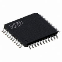
P89V662FBC,557 NXP Semiconductors, P89V662FBC,557 Datasheet - Page 67

P89V662FBC,557
Manufacturer Part Number
P89V662FBC,557
Description
IC 80C51 MCU FLASH 32K 44-TQFP
Manufacturer
NXP Semiconductors
Series
89Vr
Datasheet
1.P89V660FBC557.pdf
(89 pages)
Specifications of P89V662FBC,557
Program Memory Type
FLASH
Program Memory Size
32KB (32K x 8)
Package / Case
44-TQFP
Core Processor
8051
Core Size
8-Bit
Speed
40MHz
Connectivity
I²C, SPI, UART/USART
Peripherals
POR, PWM, WDT
Number Of I /o
36
Ram Size
1K x 8
Voltage - Supply (vcc/vdd)
4.5 V ~ 5.5 V
Oscillator Type
Internal
Operating Temperature
-40°C ~ 85°C
Processor Series
P89V6x
Core
80C51
Data Bus Width
8 bit
Data Ram Size
1 KB
Interface Type
I2C/UART
Maximum Clock Frequency
40 MHz
Number Of Programmable I/os
36
Number Of Timers
3
Operating Supply Voltage
4.5 V to 5.5 V
Maximum Operating Temperature
+ 85 C
Mounting Style
SMD/SMT
3rd Party Development Tools
PK51, CA51, A51, ULINK2
Minimum Operating Temperature
- 40 C
Lead Free Status / RoHS Status
Lead free / RoHS Compliant
For Use With
622-1001 - USB IN-CIRCUIT PROG 80C51ISP
Eeprom Size
-
Data Converters
-
Lead Free Status / Rohs Status
Lead free / RoHS Compliant
Other names
568-2435
935280832557
P89V662FBC
935280832557
P89V662FBC
Available stocks
Company
Part Number
Manufacturer
Quantity
Price
Company:
Part Number:
P89V662FBC,557
Manufacturer:
Maxim
Quantity:
260
Company:
Part Number:
P89V662FBC,557
Manufacturer:
NXP Semiconductors
Quantity:
10 000
NXP Semiconductors
P89V660_662_664_3
Product data sheet
Table 55.
Bit addressable; Reset value: 00H
Table 56.
Table 57.
Bit addressable; Reset value: 00H
Table 58.
Table 59.
Bit addressable; Reset value: 00H
Table 60.
Bit
7
6
5
4
3
2
1
0
Bit
7 to 3
2
1
0
Bit
7
6
5
4
3
2
1
0
Bit
Symbol
Bit
Symbol
Bit
Symbol
IEN0 - Interrupt enable register 0 (address A8H) bit allocation
IEN0 - Interrupt enable register 0 (address A8H) bit description
IEN1 - Interrupt enable register 1 (address E8H) bit allocation
IEN1 - Interrupt enable register 1 (address E8H) bit description
IP0 - Interrupt priority 0 low register (address B8H) bit allocation
IP0 - Interrupt priority 0 low register (address B8H) bit description
Symbol
EA
EC
ES1
ES0
ET1
EX1
ET0
EX0
Symbol
-
ES3
ES2
ET2
Symbol
PT2
PPC
PS1
PS0
PT1
PX1
PT0
PX0
PT2
EA
7
7
7
-
Rev. 03 — 10 November 2008
PPC
EC
6
6
6
-
Description
Interrupt Enable Bit: EA = 1 interrupt(s) can be serviced, EA = 0
interrupt servicing disabled.
PCA Interrupt Enable bit.
I
Serial Port Interrupt Enable
Timer 1 Overflow Interrupt Enable.
External Interrupt 1 Enable.
Timer 0 Overflow Interrupt Enable.
External Interrupt 0 Enable.
Description
Reserved for future use. Should be set to ‘0’ by user programs.
SPI Interrupt Enable.
I
Timer 2 Interrupt Enable.
Description
Timer 2 Interrupt Priority Low Bit.
PCA Interrupt Priority Low Bit.
I
Serial Port Interrupt Priority Low Bit.
Timer 1 Interrupt Priority Low Bit.
External Interrupt 1 Priority Low Bit.
Timer 0 Interrupt Priority Low Bit.
External Interrupt 0 Priority Low Bit.
2
2
2
C-bus Interrupt Enable (primary).
C-bus Interrupt Enable (secondary).
C-bus Interrupt Priority Low Bit.
ES1
PS1
5
5
5
-
80C51 with 512 B/1 kB/2 kB RAM, dual I
ES0
PS0
4
4
4
-
ET1
PT1
P89V660/662/664
3
3
3
-
EX1
ES3
PX1
2
2
2
© NXP B.V. 2008. All rights reserved.
ET0
ES2
PT0
1
1
1
2
C-bus, SPI
EX0
PX0
ET2
67 of 89
0
0
0


