P89V662FBC,557 NXP Semiconductors, P89V662FBC,557 Datasheet
P89V662FBC,557
Specifications of P89V662FBC,557
935280832557
P89V662FBC
Available stocks


Related parts for P89V662FBC,557


P89V662FBC,557 Summary of contents
Page 1
P89V660/662/664 8-bit 80C51 5 V low power 16 kB/32 kB/64 kB flash microcontroller with 512 B/1 kB/2 kB RAM, dual I Rev. 03 — 10 November 2008 1. General description The P89V660/662/664 are 80C51 microcontrollers with 16 kB/32 kB/64 kB ...
Page 2
... NXP Semiconductors I Idle mode 2.3 Comparison to the P89C660/662/664 devices I SPI interface. The P89V660/662/664 devices include an SPI interface that was not present on the P89C660/662/664 devices. I Dual I The P89C660/662/664 devices have one. I More I/O pins. The P89V660/662/664 devices have an additional four-bit I/O port, Port 4 ...
Page 3
... NXP Semiconductors 3.1 Ordering options Table 2. Type number P89V660FA P89V660FBC P89V662FA P89V662FBC P89V664FA P89V664FBC 4. Block diagram P89V660/662/664 P4[7:0] P3[7:0] P2[7:0] P1[7:0] P0[7:0] XTAL1 CRYSTAL OR RESONATOR XTAL2 Fig 1. Block diagram P89V660_662_664_3 Product data sheet 80C51 with 512 B/1 kB/2 kB RAM, dual I Ordering options ...
Page 4
... NXP Semiconductors 5. Pinning information 5.1 Pinning Fig 2. PLCC44 pin configuration P89V660_662_664_3 Product data sheet 80C51 with 512 B/1 kB/2 kB RAM, dual I P1[5]/CEX2 7 P1[6]/SCL 8 9 P1[7]/SDA RST 10 P3[0]/RXD 11 P89V660/662/664 P4[3]/ P3[1]/TXD P3[2]/INT0 14 P3[3]/INT1 15 16 ...
Page 5
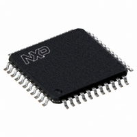
... NXP Semiconductors Fig 3. TQFP44 pin configuration P89V660_662_664_3 Product data sheet 80C51 with 512 B/1 kB/2 kB RAM, dual I P1[5]/CEX2 1 P1[6]/SCL 2 3 P1[7]/SDA RST 4 P3[0]/RXD 5 P89V660/662/664 P4[3]/ P3[1]/TXD P3[2]/INT0 8 P3[3]/INT1 9 10 P3[4]/T0/CEX3 11 P3[5]/T1/CEX4 Rev. 03 — ...
Page 6
... NXP Semiconductors 5.2 Pin description Table 3. Pin description Symbol Pin TQFP44 PLCC44 P0[0] to P0[7] P0[0]/AD0 37 43 P0[1]/AD1 36 42 P0[2]/AD2 35 41 P0[3]/AD3 34 40 P0[4]/AD4 33 39 P0[5]/AD5 32 38 P0[6]/AD6 31 37 P0[7]/AD7 30 36 P1[0] to P1[7] P1[0]/T2 ...
Page 7
... NXP Semiconductors Table 3. Pin description …continued Symbol Pin TQFP44 PLCC44 P1[4]/CEX1 44 6 P1[5]/CEX2 1 7 P1[6]/SCL 2 8 P1[7]/SDA 3 9 P2[0] to P2[7] P2[0]/ P2[1]/ P2[2]/A10 20 26 P2[3]/A11 21 27 P2[4]/A12 22 28 P2[5]/A13 23 29 P2[6]/A14 24 30 ...
Page 8
... NXP Semiconductors Table 3. Pin description …continued Symbol Pin TQFP44 PLCC44 P3[2]/INT0 8 14 P3[3]/INT1 9 15 P3[4]/T0/CEX3 10 16 P3[5]/T1/CEX4 11 17 P3[6]/ P3[7]/ P4[0] to P4[3] P4[0]/SCL_1 SCK P4[1]/SDA_1 MISO P4[2]/MOSI 39 1 P4[3]/ PSEN 26 32 RST P89V660_662_664_3 Product data sheet ...
Page 9
... NXP Semiconductors Table 3. Pin description …continued Symbol Pin TQFP44 PLCC44 ALE/PROG 27 33 XTAL1 15 21 XTAL2 [1] ALE loading issue: When ALE pin experiences higher loading (>30 pF) during the reset, the microcontroller may accidentally enter into modes other than normal working mode. The solution is to add a pull-up resistor ...
Page 10
... NXP Semiconductors 6. Functional description 6.1 Special function registers Remark: SFR accesses are restricted in the following ways: • User must not attempt to access any SFR locations not defined. • Accesses to any defined SFR locations must be strictly for the functions for the SFRs. ...
Page 11
Table 4. Special function registers * indicates Special Function Registers (SFRs) that are bit addressable. Name Description Bit address ACC* Accumulator AUXR Auxiliary function register AUXR1 Auxiliary function register 1 Bit address B* B register CCAP0H Module 0 Capture HIGH ...
Page 12
Table 4. Special function registers …continued * indicates Special Function Registers (SFRs) that are bit addressable. Name Description Bit address IEN0* Interrupt Enable 0 Bit address IEN1* Interrupt Enable 1 Bit address IP0* Interrupt Priority 0 IP0H Interrupt Priority 0 ...
Page 13
Table 4. Special function registers …continued * indicates Special Function Registers (SFRs) that are bit addressable. Name Description SADEN Serial Port Address Enable Bit address SPCR SPI Control Register SPSR SPI Configuration Register SPDAT SPI Data SP Stack Pointer 2 ...
Page 14
... NXP Semiconductors 6.2 Memory organization The various P89V660/662/664 memory spaces are as follows: • DATA 128 B of internal data memory space (00H:7FH) accessed via direct or indirect addressing, using instructions other than MOVX and MOVC. All or part of the Stack may be in this area. ...
Page 15
... NXP Semiconductors for the 89V662, above 6FFH for the 89V664) will access external off-chip memory and will perform in the same way as the standard 8051, with P0 and P2 as data/address bus, and P3[6] and P3[7] as write and read timing signals. Table 6. Bit When EXTRAM = 0, MOVX @Ri and MOVX @DPTR will be similar to the standard 8051. ...
Page 16
... NXP Semiconductors 2FFH 000H Fig 4. Internal and external data memory structure 6.2.2 Dual data pointers The device has two 16-bit data pointers. The DPTR Select (DPS) bit in AUXR1 determines which of the two data pointers is accessed. When DPS = 0, DPTR0 is selected; when DPS = 1, DPTR1 is selected. Quickly switching between the two data ...
Page 17
... NXP Semiconductors Fig 5. Dual data pointer organization Table 8. Not bit addressable; Reset value 00H Bit Symbol Table 9. Bit 6.2.3 Reset At initial power-up, the port pins will random state until the oscillator has started and the internal reset algorithm has weakly pulled all pins high. Powering up the device without a valid reset could cause the MCU to start executing instructions from an indeterminate location. Such undefi ...
Page 18
... NXP Semiconductors Fig 6. Power-on reset circuit 6.3 Flash memory 6.3.1 Flash organization The P89V660/662/664 program memory consists of a 16/32/64 kB block for user code. The flash can be read or written in bytes and can be erased in 128 pages. A chip erase function will erase the entire user code memory and its associated security bits. There are three methods of erasing or programming the fl ...
Page 19
... NXP Semiconductors 6.3.3 Boot block When the microcontroller programs its own flash memory, all of the low level details are handled by code (bootloader) that is contained in a Boot block. A user program calls the common entry point in the Boot block with appropriate parameters to accomplish the desired operation ...
Page 20
... NXP Semiconductors based on the oscillator frequency. The ISP feature requires that an initial character (an uppercase U) be sent to the P89V660/662/664 to establish the baud rate. The ISP firmware provides auto-echo of received characters. Once baud rate initialization has been performed, the ISP firmware will only accept Intel Hex-type records. Intel Hex ...
Page 21
... NXP Semiconductors Table 11. Record type 03 P89V660_662_664_3 Product data sheet 80C51 with 512 B/1 kB/2 kB RAM, dual I ISP hex record formats …continued Command/data function Miscellaneous Write Functions :nnxxxx03ffssddcc Where number of bytes in the record xxxx = required field but value is a ‘don’t care’ ...
Page 22
... NXP Semiconductors Table 11. Record type P89V660_662_664_3 Product data sheet 80C51 with 512 B/1 kB/2 kB RAM, dual I ISP hex record formats …continued Command/data function Display Device Data or Blank Check :05xxxx04sssseeeeffcc Where 05 = number of bytes in the record xxxx = required field but value is a ‘don’t care’ ...
Page 23
... NXP Semiconductors 6.3.8 IAP method Several IAP calls are available for use by an application program to permit selective erasing, reading and programming of flash pages, security bits, security bits, Status bit, and device id. All calls are made through a common interface, PGM_MTP. The programming functions are selected by setting up the microcontroller’s registers before making a call to PGM_MTP at FFF0H ...
Page 24
... NXP Semiconductors Table 12. IAP function Erase Status bit and Boot vector Program Security bits Program Status bit, Boot vector, 6x/12x bit Read Security bits, Status bit, Boot vector Erase page 2 6.4 I C-bus interface 2 The I C-bus uses two wires, Serial Clock (SCL) and Serial Data (SDA) to transfer information between devices connected to the bus, and has the following features: • ...
Page 25
... NXP Semiconductors • Multimaster bus (no central master) • Arbitration between simultaneously transmitting masters without corruption of serial data on the bus • Serial clock synchronization allows devices with different bit rates to communicate via one serial bus • Serial clock synchronization can be used as a handshake mechanism to suspend and resume serial transfer • ...
Page 26
... NXP Semiconductors 2 6.4.1 I C-bus data register S1DAT register contains the data to be transmitted or the data received. The CPU can read and write to this 8-bit register while it is not in the process of shifting a byte. Thus this register should only be accessed when the SI bit is set. Data in S1DAT remains stable as long as the SI bit is set. Data in S1DAT is always shifted from right to left: the fi ...
Page 27
... NXP Semiconductors Table 15. Bit Symbol Reset 2 Table 16. I C-bus control register (S1CON - address D8H) bit description Bit Symbol Description 7,1,0 CR2:0 SCL clock selection. See 2 AA The Assert Acknowledge Flag. When set acknowledge (LOW-state to SDA) will be returned during the acknowledge clock pulse on the SCL line on the following situations: 1. The ‘ ...
Page 28
... NXP Semiconductors 2 Table 17. I C-bus clock rates …continued CR2:0 6-clock mode 6 MHz 12 MHZ 101 100 200 110 200 400 111 0.49 < 62.5 0.98 < 50.0 2 6.4.4 I C-bus status register This is a read-only register. It contains the status code of the I three bits are always 0. There are 26 possible status codes. When the code is F8H, there is no relevant information available and SI bit is not set. All other 25 status codes correspond to defi ...
Page 29
... NXP Semiconductors 2 The I C-bus will enter Master Transmitter mode by setting the STA bit. The I will send the START condition as soon as the bus is free. After the START condition is transmitted, the SI bit is set, and the status code in S1STA should be 08H. This status code must be used to vector to an interrupt service routine where the user should load the slave address to S1DAT and data direction bit (SLA+W) ...
Page 30
... NXP Semiconductors S SLA logic 0 = write logic 1 = read from master to slave from slave to master Fig 10. A Master Receiver switches to Master Transmitter after sending Repeated Start. 6.4.5.3 Slave receiver mode In the Slave Receiver mode, data bytes are received from a master transmitter. To initialize the Slave Receiver mode, the user should write the slave address to the Slave Address Register (S1ADR) and the I confi ...
Page 31
... NXP Semiconductors STOP conditions are recognized as the beginning and end of a serial transfer given application, the C-bus hardware looks for its own slave address and the general call address. If one of these addresses is detected, an interrupt is requested. When the microcontrollers wishes to become the bus master, the hardware waits until the bus is free before the master mode is entered so that a possible slave action is not interrupted ...
Page 32
... NXP Semiconductors P1[7]/SDA P1[6]/SCL Fig 13. I P89V660_662_664_3 Product data sheet 80C51 with 512 B/1 kB/2 kB RAM, dual I P1[7] INPUT FILTER OUTPUT STAGE INPUT FILTER OUTPUT STAGE timer 1 overflow P1[6] I2CON I2SCLH I2SCLL status bus I2STAT 2 C-bus serial interface block diagram Rev. 03 — ...
Page 33
... NXP Semiconductors Table 22. Master transmitter mode Status code Status of the 2 (S1STA) I C-bus hardware 08H A START condition has been transmitted. 10H A repeat START condition has been transmitted. 18H SLA+W has been transmitted; ACK has been received. 20H SLA+W has been transmitted; NOT-ACK has been received ...
Page 34
... NXP Semiconductors Table 22. Master transmitter mode Status code Status of the 2 (S1STA) I C-bus hardware 30H Data byte in S1DAT has been transmitted, NOT ACK has been received. 38H Arbitration lost in SLA+R/W or data bytes. Table 23. Master Receiver mode Status code Status of the 2 (S1STA) I C-bus ...
Page 35
... NXP Semiconductors Table 23. Master Receiver mode Status code Status of the 2 (S1STA) I C-bus hardware 50H Data byte has been received; ACK has been returned. 58H Data byte has been received; NOT ACK has been returned. Table 24. Slave Receiver mode Status code Status of the ...
Page 36
... NXP Semiconductors Table 24. Slave Receiver mode Status code Status of the 2 (S1STA) I C-bus hardware 88H Previously addressed with own SLA address; Data has been received; NOT ACK has been returned. 90H Previously addressed with General call; Data has been received; ACK has been returned ...
Page 37
... NXP Semiconductors Table 24. Slave Receiver mode Status code Status of the 2 (S1STA) I C-bus hardware A0H A STOP condition or repeated START condition has been received while still addressed as SLA/REC or SLA/TRX. Table 25. Slave transmitter mode Status code Status of the 2 (S1STA) I C-bus hardware A8H Own SLA+R has been received ...
Page 38
... NXP Semiconductors Table 25. Slave transmitter mode Status code Status of the 2 (S1STA) I C-bus hardware C0H Data byte in S1DAT has been transmitted; NOT ACK has been received. C8H Last data byte in S1DAT has been transmitted (AA = 0); ACK has been received. 6.5 Timers/counters 0 and 1 The two 16-bit Timer/Counter registers: Timer 0 and Timer 1 can be confi ...
Page 39
... NXP Semiconductors In the ‘Counter’ function, the register is incremented in response to a 1-to-0 transition at its corresponding external input pin T1. In this function, the external input is sampled once every machine cycle. When the samples show a high in one cycle and a low in the next cycle, the count is incremented ...
Page 40
... NXP Semiconductors Table 28 Table 29. Bit addressable; Reset value: 0000 0000B; Reset source(s): any reset Bit Symbol Table 30. Bit 6.5.1 Mode 0 Putting either Timer into Mode 0 makes it look like an 8048 Timer, which is an 8-bit Counter with a fixed divide-by-32 prescaler. P89V660_662_664_3 Product data sheet ...
Page 41
... NXP Semiconductors osc/6 Tn pin TnGate INTn pin Fig 14. Timer/Counter Mode 0 (13-bit counter) In this mode, the Timer register is configured as a 13-bit register. As the count rolls over from all 1s to all 0s, it sets the Timer interrupt flag TFn. The count input is enabled to the Timer when TRn = 1 and either GATE = 0 or INTn = 1 ...
Page 42
... NXP Semiconductors Tn pin TnGate INTn pin Fig 16. Timer/Counter Mode 2 (8-bit auto-reload) 6.5.4 Mode 3 When timer Mode stopped (holds its count). The effect is the same as setting TR1 = 0. Timer 0 in Mode 3 establishes TL0 and TH0 as two separate 8-bit counters. The logic for Mode 3 and Timer 0 is shown in T0GATE, TR0, INT0, and TF0 ...
Page 43
... NXP Semiconductors Table 31. RCLK+TCLK Table 32. Bit addressable; Reset value: 00H Bit Symbol Table 33. Bit Table 34. Not bit addressable; Reset value: XX00 0000B Bit Symbol P89V660_662_664_3 Product data sheet 80C51 with 512 B/1 kB/2 kB RAM, dual I Timer 2 operating mode CP/RL2 TR2 T2CON - Timer/Counter 2 control register (address C8H) bit allocation ...
Page 44
... NXP Semiconductors Table 35. Bit 6.6.1 Capture mode In the Capture mode there are two options which are selected by bit EXEN2 in T2CON. If EXEN2 = 0 Timer 16-bit timer or counter (as selected by C/T2 in T2CON) which upon overflowing sets bit TF2, the Timer 2 overflow bit. The capture mode is illustrated in ...
Page 45
... NXP Semiconductors 6.6.2 Auto-reload mode (up or down-counter) In the 16-bit auto-reload mode, Timer 2 can be configured as either a timer or counter (via C/T2 in T2CON), then programmed to count up or down. The counting direction is determined by bit DCEN (Down-counter Enable) which is located in the T2MOD register (see Table 34 counting up ...
Page 46
... NXP Semiconductors In Figure T2EX to control the direction of count. When a logic ‘1’ is applied at pin T2EX Timer 2 will count up. Timer 2 will overflow at 0FFFFH and set the TF2 flag, which can then generate an interrupt, if the interrupt is enabled. This timer overflow also causes the 16-bit value in RCAP2L and RCAP2H to be reloaded into the timer registers TL2 and TH2 ...
Page 47
... NXP Semiconductors 6.6.4 Baud rate generator mode Bits TCLK and/or RCLK in T2CON allow the UART) transmit and receive baud rates to be derived from either Timer 1 or Timer 2 (See Timer 1 is used as the UART transmit baud rate generator. When TCLK = 1, Timer 2 is used as the UART transmit baud rate generator ...
Page 48
... NXP Semiconductors baud rate generator mode. Also if the EXEN2 (T2 external enable flag) is set, a 1-to-0 transition in T2EX (Timer/counter 2 trigger input) will set EXF2 (T2 external flag) but will not cause a reload from (RCAP2H, RCAP2L) to (TH2,TL2). Therefore when Timer use as a baud rate generator, T2EX can be used as an additional external interrupt, if needed ...
Page 49
... NXP Semiconductors 6.7.1 Mode 0 Serial data enters and exits through RXD and TXD outputs the shift clock. Only 8 bits are transmitted or received, LSB first. The baud rate is fixed at UART configured to operate in this mode outputs serial clock on TXD line no matter whether it sends or receives data on RXD line. ...
Page 50
... NXP Semiconductors Table 38. Bit Table 39. SM0, SM1 6.7.5 Framing error Framing error (FE) is reported in the SCON.7 bit if SMOD0 (PCON. SMOD0 = 0, SCON.7 is the SM0 bit for the UART recommended that SM0 is set up before SMOD0 is set to ‘1’. 6.7.6 More about UART mode 1 Reception is initiated by a detected 1-to-0 transition at RXD ...
Page 51
... NXP Semiconductors The signal to load SBUF and RB8, and to set RI, will be generated if, and only if, the following conditions are met at the time the final shift pulse is generated: ( and (b) Either SM2 = 0, or the received 9th data bit = 1. If either of these conditions is not met, the received frame is irretrievably lost, and RI is not set. If both conditions are met, the received 9th data bit goes into RB8, and the fi ...
Page 52
... NXP Semiconductors Fig 22. Schemes used by the UART to detect ‘given’ and ‘broadcast’ addresses when The following examples will help to show the versatility of this scheme. Example 1, slave 0: SADDR = 1100 0000 SADEN = 1111 1101 --------------------------------------------------- - Given = 1100 00X0 Example 2, slave 1: SADDR = 1100 0000 ...
Page 53
... NXP Semiconductors In a more complex system the following could be used to select slaves 1 and 2 while excluding slave 0: Example 1, slave 0: SADDR = 1100 0000 SADEN = 1111 1001 --------------------------------------------------- - Given = 1100 0XX0 Example 2, slave 1: SADDR = 1110 0000 SADEN = 1111 1010 --------------------------------------------------- - Given = 1110 0X0X Example 2, slave 2: SADDR = 1100 0000 ...
Page 54
... NXP Semiconductors pin is the clock output and input for the master and slave modes, respectively. The SPI clock generator will start following a write to the master devices SPI data register. The written data is then shifted out of the MOSI pin on the master device into the MOSI pin of the slave device. Following a complete transmission of one byte of data, the SPI clock generator is stopped and the SPIF fl ...
Page 55
... NXP Semiconductors Table 41. Bit Table 42. SPR1 Table 43. Bit addressable; Reset source(s): any reset; Reset value: 0000 0000B Bit Symbol Table 44. Bit SCK (CPOL = 0) SCK (CPOL = 1) Fig 24. SPI transfer format with CPHA = 0 P89V660_662_664_3 Product data sheet 80C51 with 512 B/1 kB/2 kB RAM, dual I ...
Page 56
... NXP Semiconductors SCK (CPOL = 0) SCK (CPOL = 1) Fig 25. SPI transfer format with CPHA = 1 6.9 Watchdog timer The WDT is intended as a recovery method in situations where the CPU may be subjected to software upset. The WDT consists of a 14-bit counter and the WatchDog Timer Reset (WDTRST) SFR. The WDT is disabled at reset. To enable the WDT, the user must write 01EH and 0E1H, in sequence, to the WDTRST SFR ...
Page 57
... NXP Semiconductors time base for PCA modules Fig 26. PCA In the CMOD SFR there are three additional bits associated with the PCA. They are CIDL which allows the PCA to stop during Idle mode, WDTE which enables or disables the Watchdog function on module 4, and ECF which when set causes an interrupt and the PCA overfl ...
Page 58
... NXP Semiconductors The next two bits CAPN (CCAPMn.4) and CAPP (CCAPMn.5) determine the edge that a capture input will be active on. The CAPN bit enables the negative edge, and the CAPP bit enables the positive edge. If both bits are set both edges will be enabled and a capture will occur for either transition ...
Page 59
... NXP Semiconductors Table 46. Bit Table 47. CPS1 Table 48. Bit addressable; Reset value: 00H Bit Symbol Table 49. Bit P89V660_662_664_3 Product data sheet 80C51 with 512 B/1 kB/2 kB RAM, dual I CMOD - PCA counter mode register (address C1H) bit description Symbol Description CIDL Counter Idle Control: CIDL = 0 programs the PCA Counter to continue functioning during Idle mode ...
Page 60
... NXP Semiconductors Table 50. Not bit addressable; Reset value: 00H Bit Symbol Table 51. Bit Table 52. PCA module modes (CCAPMn register) ECOMn CAPPn CAPNn 6.10.1 PCA capture mode To use one of the PCA modules in the capture mode CCAPM bits CAPN and CAPP for that module must be set. The external CEX input for the module (on port 1) is sampled for a transition. When a valid transition occurs the PCA hardware loads the value of the PCA counter registers (CH and CL) into the module’ ...
Page 61
... NXP Semiconductors CF CR CEXn - ECOMn 0 Fig 28. PCA capture mode If the CCFn bit for the module in the CCON SFR and the ECCFn bit in the CCAPMn SFR are set then an interrupt will be generated. 6.10.2 16-bit software timer mode The PCA modules can be used as software timers and MAT bits in the modules CCAPMn register. The PCA timer will be compared to the module’ ...
Page 62
... NXP Semiconductors write to CCAPnH reset write to CCAPnL enable 0 1 Fig 29. PCA compare mode 6.10.3 High-speed output mode In this mode toggle each time a match occurs between the PCA counter and the module’s capture registers. To activate this mode the TOG, MAT, and ECOM bits in the module’s CCAPMn SFR must be set ...
Page 63
... NXP Semiconductors write to reset CCAPnH write to CCAPnL enable 0 1 Fig 30. PCA high-speed output mode 6.10.4 Pulse width modulator mode All of the PCA modules can be used as PWM outputs depends on the source for the PCA timer. enable - ECOMn CAPPn 1 Fig 31. PCA PWM mode All of the modules will have the same frequency of output because they all share one and only PCA timer ...
Page 64
... NXP Semiconductors value in the module’s CCAPnL SFR the output will be low, when it is equal to or greater than the output will be high. When CL overflows from FF to 00, CCAPnL is reloaded with the value in CCAPnH. This allows updating the PWM without glitches. The PWM and ECOM bits in the module’ ...
Page 65
... NXP Semiconductors 6.11 Security bits The security bits protects against software piracy and prevents the contents of the flash from being read by unauthorized parties in Parallel Programmer mode and ISP mode. Since the end application might need to erase pages and read from the code memory, the security bits have no effect in IAP mode. However, the security bits’ ...
Page 66
... NXP Semiconductors 0 INT0 IT0 1 SPIF SPIE TF0 0 INT1 IT1 1 TF1 ECF CF CCFn ECCFn RI TI TF2 EXF2 2 I C-bus (primary C-bus (secondary) Fig 32. Interrupt structure P89V660_662_664_3 Product data sheet 80C51 with 512 B/1 kB/2 kB RAM, dual I IP/IPH/IPA/IPAH IE and IEA registers IE0 IE1 ...
Page 67
... NXP Semiconductors Table 55. Bit addressable; Reset value: 00H Bit Symbol Table 56. Bit Table 57. Bit addressable; Reset value: 00H Bit Symbol Table 58. Bit Table 59. Bit addressable; Reset value: 00H Bit Symbol Table 60. Bit P89V660_662_664_3 Product data sheet 80C51 with 512 B/1 kB/2 kB RAM, dual I ...
Page 68
... NXP Semiconductors Table 61. Not bit addressable; Reset value: 00H Bit Symbol Table 62. Bit Table 63. Bit addressable; Reset value: 00H Bit Symbol Table 64. Bit Table 65. Not bit addressable; Reset value: 00H Bit Symbol Table 66. Bit 6.13 Power-saving modes The device provides two power saving modes of operation for applications where power consumption is critical ...
Page 69
... NXP Semiconductors 6.13.1 Idle mode Idle mode is entered setting the IDL bit in the PCON register. In Idle mode, the program counter is stopped. The system clock continues to run and all interrupts and peripherals remain active. The on-chip RAM and the special function registers hold their data during this mode ...
Page 70
... NXP Semiconductors 6.14 System clock and clock options 6.14.1 Clock input options and recommended capacitor values for the oscillator Shown in amplifier (XTAL1, XTAL2), which can be configured for use as an on-chip oscillator. When driving the device from an external clock source, XTAL2 should be left disconnected and XTAL1 should be driven ...
Page 71
... NXP Semiconductors 7. Limiting values Table 69. Limiting values In accordance with the Absolute Maximum Rating System (IEC 60134). Parameters are valid over operating temperature range unless otherwise specified. All voltages are with respect to V otherwise noted. Symbol Parameter T bias ambient temperature amb(bias) ...
Page 72
... NXP Semiconductors Table 70. Static characteristics + 4 5 amb DD Symbol Parameter I HIGH-LOW transition current THL I input leakage current LI R pull-down resistance pd C input capacitance iss I operating supply current DD(oper) I Idle mode supply current DD(idle) I Power-down mode supply DD(pd) current [1] This parameter is measured only for initial qualification and after a design or process change that could affect this parameter. ...
Page 73
... NXP Semiconductors (mA (1) Maximum active I DD (2) Maximum idle I DD (3) Typical active I DD (4) Typical idle I DD Fig 35. I vs. frequency DD P89V660_662_664_3 Product data sheet 80C51 with 512 B/1 kB/2 kB RAM, dual Rev. 03 — 10 November 2008 P89V660/662/664 2 002aaa813 (1) (2) (3) ( internal clock frequency (MHz) © NXP B.V. 2008. All rights reserved. ...
Page 74
... NXP Semiconductors 9. Dynamic characteristics Table 71. Dynamic characteristics Over operating conditions: load capacitance for Port 0, ALE, and PSEN = 100 pF; load capacitance for all other outputs = + 4 5 amb DD Symbol Parameter f oscillator frequency osc t ALE pulse width LHLL t address valid to ALE LOW time AVLL ...
Page 75
... NXP Semiconductors 9.1 Explanation of symbols Each timing symbol has 5 characters. The first character is always a ‘T’ (stands for time). The other characters, depending on their positions, stand for the name of a signal or the logical status of that signal. The following is a list of all the characters and what they stand for. A — ...
Page 76
... NXP Semiconductors ALE PSEN RD t LLAX t AVLL port 0 from RI to DPL port 2 Fig 37. External data memory read cycle t LHLL ALE PSEN WR t AVLL from RI or DPL port 0 port 2 Fig 38. External data memory write cycle P89V660_662_664_3 Product data sheet 80C51 with 512 B/1 kB/2 kB RAM, dual I ...
Page 77
... NXP Semiconductors Table 72. External clock drive Symbol Parameter f oscillator frequency osc T clock cycle time cy(clk) t clock HIGH time CHCX t clock LOW time CLCX t clock rise time CLCH t clock fall time CHCL Fig 39. External clock drive waveform Table 73. Serial port timing Symbol ...
Page 78
... NXP Semiconductors instruction ALE clock t QVXH output data write to SBUF t XHDV input data clear RI Fig 40. Shift register mode timing waveforms 2 Table 74. I C-bus interface timing (12-clock mode) Symbol Parameter t hold time (repeated) START condition HD;STA t LOW period of the SCL clock LOW ...
Page 79
... NXP Semiconductors START or repeated START condition t SCL (input/ output) t fDA t rCL SDA (input/ output HD;STA LOW 2 Fig 41. I C-bus interface timing Table 75. SPI interface timing Symbol Parameter f SPI operating frequency SPI T SPI cycle time SPICYC t SPI enable lead time SPILEAD t SPI enable lag time ...
Page 80
... NXP Semiconductors SS SPICLK (CPOL = 0) (output) SPICLK (CPOL = 1) (output) MISO (input) t MOSI SPIF (output) Fig 42. SPI master timing (CPHA = 0) SS SPICLK (CPOL = 0) (output) SPICLK (CPOL = 1) (output) MISO (input) t SPIF MOSI (output) Fig 43. SPI master timing (CPHA = 1) P89V660_662_664_3 Product data sheet 80C51 with 512 B/1 kB/2 kB RAM, dual I ...
Page 81
... NXP Semiconductors SS t SPIR t SPILEAD SPICLK (CPOL = 0) (input) t SPIF SPICLK (CPOL = 1) (input) t SPIA MISO (output) t SPIDSU MOSI (input) Fig 44. SPI slave timing (CPHA = SPIR t SPILEAD SPICLK (CPOL = 0) (input) t SPIF SPICLK (CPOL = 1) (input) t SPIOH t SPIDV t SPIA MISO not defined (output) MOSI (input) Fig 45 ...
Page 82
... NXP Semiconductors Fig 46. Test load example Fig 47. I Fig 48. I P89V660_662_664_3 Product data sheet 80C51 with 512 B/1 kB/2 kB RAM, dual I to DUT V DD (n.c.) clock signal All other pins disconnected test condition, active mode DD (n.c.) clock signal All other pins disconnected ...
Page 83
... NXP Semiconductors Fig 49. I P89V660_662_664_3 Product data sheet 80C51 with 512 B/1 kB/2 kB RAM, dual RST (n.c.) XTAL2 XTAL1 V SS All other pins disconnected test condition, Power-down mode DD Rev. 03 — 10 November 2008 P89V660/662/664 = DUT 002aaa558 2 C-bus, SPI © NXP B.V. 2008. All rights reserved. ...
Page 84
... NXP Semiconductors 10. Package outline TQFP44: plastic thin quad flat package; 44 leads; body 1 pin 1 index DIMENSIONS (mm are the original dimensions) A UNIT max. 0.15 1.05 1.2 mm 0.25 0.05 0.95 Note 1. Plastic or metal protrusions of 0.25 mm maximum per side are not included. OUTLINE VERSION IEC ...
Page 85
... NXP Semiconductors PLCC44: plastic leaded chip carrier; 44 leads pin 1 index DIMENSIONS (mm dimensions are derived from the original inch dimensions UNIT max. min. 4.57 0.53 mm 0.51 0.25 3.05 4.19 0.33 0.180 0.021 inches 0.02 0.01 0.12 0.165 0.013 Note 1. Plastic or metal protrusions of 0.25 mm (0.01 inch) maximum per side are not included. ...
Page 86
... NXP Semiconductors 11. Abbreviations Table 76. Acronym ALE CPU DUT EPROM EMI MCU PWM RAM RC SFR SPI UART P89V660_662_664_3 Product data sheet 80C51 with 512 B/1 kB/2 kB RAM, dual I Acronym list Description Address Latch Enabled Central Processing Unit Device Under Test Erasable Programmable Read-Only Memory ...
Page 87
... NXP Semiconductors 12. Revision history Table 77. Revision history Document ID Release date P89V660_662_664_3 20081110 • Modifications: Section 2.2 “Additional P89V660_662_664_2 20080129 P89V660_662_664_1 20070502 P89V660_662_664_3 Product data sheet 80C51 with 512 B/1 kB/2 kB RAM, dual I Data sheet status Change notice Product data sheet - features” ...
Page 88
... Right to make changes — NXP Semiconductors reserves the right to make changes to information published in this document, including without limitation specifications and product descriptions, at any time and without notice ...
Page 89
... NXP Semiconductors 15. Contents 1 General description . . . . . . . . . . . . . . . . . . . . . . 1 2 Features . . . . . . . . . . . . . . . . . . . . . . . . . . . . . . . 1 2.1 Principal features . . . . . . . . . . . . . . . . . . . . . . . 1 2.2 Additional features . . . . . . . . . . . . . . . . . . . . . . 1 2.3 Comparison to the P89C660/662/664 devices . 2 3 Ordering information . . . . . . . . . . . . . . . . . . . . . 2 3.1 Ordering options . . . . . . . . . . . . . . . . . . . . . . . . 3 4 Block diagram . . . . . . . . . . . . . . . . . . . . . . . . . . 3 5 Pinning information . . . . . . . . . . . . . . . . . . . . . . 4 5.1 Pinning . . . . . . . . . . . . . . . . . . . . . . . . . . . . . . . 4 5.2 Pin description . . . . . . . . . . . . . . . . . . . . . . . . . 6 6 Functional description . . . . . . . . . . . . . . . . . . 10 6.1 Special function registers . . . . . . . . . . . . . . . . 10 6 ...