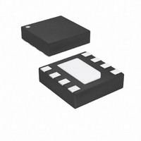
ATTINY9-MAHR Atmel, ATTINY9-MAHR Datasheet - Page 87

ATTINY9-MAHR
Manufacturer Part Number
ATTINY9-MAHR
Description
IC MCU AVR 1K FLASH 8UDFN
Manufacturer
Atmel
Series
AVR® ATtinyr
Datasheet
1.ATTINY9-MAHR.pdf
(169 pages)
Specifications of ATTINY9-MAHR
Package / Case
8-UDFN Exposed Pad
Voltage - Supply (vcc/vdd)
1.8 V ~ 5.5 V
Operating Temperature
-40°C ~ 85°C
Speed
12MHz
Number Of I /o
4
Core Processor
AVR
Program Memory Type
FLASH
Ram Size
32 x 8
Program Memory Size
1KB (1K x 8)
Oscillator Type
Internal
Peripherals
POR, PWM, WDT
Core Size
8-Bit
Lead Free Status / RoHS Status
Lead free / RoHS Compliant
Eeprom Size
-
Data Converters
-
Connectivity
-
Lead Free Status / Rohs Status
Details
Available stocks
Company
Part Number
Manufacturer
Quantity
Price
Company:
Part Number:
ATTINY9-MAHR
Manufacturer:
ST
Quantity:
101
- Current page: 87 of 169
- Download datasheet (5Mb)
8127D–AVR–02/10
switched on by setting the ADEN bit in ADCSRA. The prescaler keeps running for as long as the
ADEN bit is set, and is continuously reset when ADEN is low.
When initiating a single ended conversion by setting the ADSC bit in ADCSRA, the conversion
starts at the following rising edge of the ADC clock cycle.
A normal conversion takes 13 ADC clock cycles, as summarised in
first conversion after the ADC is switched on (ADEN in ADCSRA is set) takes 25 ADC clock
cycles in order to initialize the analog circuitry. See
Figure 13-4. ADC Timing Diagram, First Conversion (Single Conversion Mode)
The actual sample-and-hold takes place 3 ADC clock cycles after the start of a normal conver-
sion and 16 ADC clock cycles after the start of a first conversion. See
conversion is complete, the result is written to the ADC Data Registers, and ADIF is set. In Sin-
gle Conversion mode, ADSC is cleared simultaneously. The software may then set ADSC again,
and a new conversion will be initiated on the first rising ADC clock edge.
Figure 13-5. ADC Timing Diagram, Single Conversion
When Auto Triggering is used, the prescaler is reset when the trigger event occurs. See
13-6. This assures a fixed delay from the trigger event to the start of conversion. In this mode,
the sample-and-hold takes place two ADC clock cycles after the rising edge on the trigger
source signal. Three additional CPU clock cycles are used for synchronization logic.
Cycle Number
ADC Clock
ADEN
ADSC
ADIF
ADCL
Cycle Number
ADC Clock
ADSC
ADIF
ADCL
Update
MUX
Update
MUX
1
1
2
2
12
Sample & Hold
3
13
4
14
5
15
Sample & Hold
6
16
First Conversion
7
17
One Conversion
18
8
Figure
19
9
20
13-4.
10
21
11
22
Table 13-1 on page
ATtiny4/5/9/10
12
23
Conversion
Complete
24
13
Figure
Conversion
Complete
25
Update
MUX
13-5. When a
Conversion Result
Update
Next Conversion
MUX
1
Conversion Result
Next
Conversion
1
2
88. The
2
Figure
3
3
87
Related parts for ATTINY9-MAHR
Image
Part Number
Description
Manufacturer
Datasheet
Request
R

Part Number:
Description:
Manufacturer:
Atmel Corporation
Datasheet:

Part Number:
Description:
IC MCU AVR 1KB FLASH SOT-23-6
Manufacturer:
Atmel
Datasheet:

Part Number:
Description:
IC MCU AVR 1KB FLASH SOT-23-6
Manufacturer:
Atmel
Datasheet:

Part Number:
Description:
IC MCU AVR 1K FLASH 8UDFN
Manufacturer:
Atmel
Datasheet:

Part Number:
Description:
DEV KIT FOR AVR/AVR32
Manufacturer:
Atmel
Datasheet:

Part Number:
Description:
INTERVAL AND WIPE/WASH WIPER CONTROL IC WITH DELAY
Manufacturer:
ATMEL Corporation
Datasheet:

Part Number:
Description:
Low-Voltage Voice-Switched IC for Hands-Free Operation
Manufacturer:
ATMEL Corporation
Datasheet:

Part Number:
Description:
MONOLITHIC INTEGRATED FEATUREPHONE CIRCUIT
Manufacturer:
ATMEL Corporation
Datasheet:

Part Number:
Description:
AM-FM Receiver IC U4255BM-M
Manufacturer:
ATMEL Corporation
Datasheet:

Part Number:
Description:
Monolithic Integrated Feature Phone Circuit
Manufacturer:
ATMEL Corporation
Datasheet:

Part Number:
Description:
Multistandard Video-IF and Quasi Parallel Sound Processing
Manufacturer:
ATMEL Corporation
Datasheet:

Part Number:
Description:
High-performance EE PLD
Manufacturer:
ATMEL Corporation
Datasheet:


