ATTINY9-MAHR Atmel, ATTINY9-MAHR Datasheet - Page 54
ATTINY9-MAHR
Manufacturer Part Number
ATTINY9-MAHR
Description
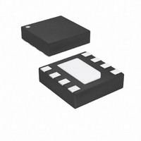
IC MCU AVR 1K FLASH 8UDFN
Manufacturer
Atmel
Series
AVR® ATtinyr
Datasheet
1.ATTINY9-MAHR.pdf
(169 pages)
Specifications of ATTINY9-MAHR
Package / Case
8-UDFN Exposed Pad
Voltage - Supply (vcc/vdd)
1.8 V ~ 5.5 V
Operating Temperature
-40°C ~ 85°C
Speed
12MHz
Number Of I /o
4
Core Processor
AVR
Program Memory Type
FLASH
Ram Size
32 x 8
Program Memory Size
1KB (1K x 8)
Oscillator Type
Internal
Peripherals
POR, PWM, WDT
Core Size
8-Bit
Lead Free Status / RoHS Status
Lead free / RoHS Compliant
Eeprom Size
-
Data Converters
-
Connectivity
-
Lead Free Status / Rohs Status
Details
Available stocks
Company
Part Number
Manufacturer
Quantity
Price
Company:

Part Number:
ATTINY9-MAHR
Manufacturer:
ST
Quantity:
101


11.2.1
11.2.2
54
ATtiny4/5/9/10
Registers
Definitions
A simplified block diagram of the 16-bit Timer/Counter is shown in
actual placement of I/O pins, refer to
Registers, including I/O bits and I/O pins, are shown in bold. The device-specific I/O Register
and bit locations are listed in the
Most register and bit references in this section are written in general form. A lower case “n”
replaces the Timer/Counter number, and a lower case “x” replaces the Output Compare unit
channel. However, when using the register or bit defines in a program, the precise form must be
used, i.e., TCNT0 for accessing Timer/Counter0 counter value and so on.
The Timer/Counter (TCNT0), Output Compare Registers (OCR0A/B), and Input Capture Regis-
ter (ICR0) are all 16-bit registers. Special procedures must be followed when accessing the 16-
bit registers. These procedures are described in the section
page
access restrictions. Interrupt requests (abbreviated to Int.Req. in the figure) signals are all visible
in the Timer Interrupt Flag Register (TIFR). All interrupts are individually masked with the Timer
Interrupt Mask Register (TIMSK). TIFR and TIMSK are not shown in the figure.
The Timer/Counter can be clocked internally, via the prescaler, or by an external clock source on
the T0 pin. The Clock Select logic block controls which clock source and edge the Timer/Counter
uses to increment (or decrement) its value. The Timer/Counter is inactive when no clock source
is selected. The output from the Clock Select logic is referred to as the timer clock (clkT
The double buffered Output Compare Registers (OCR0A/B) are compared with the Timer/Coun-
ter value at all time. The result of the compare can be used by the Waveform Generator to
generate a PWM or variable frequency output on the Output Compare pin (OC0A/B). See
put Compare Units” on page
Flag (OCF0A/B) which can be used to generate an Output Compare interrupt request.
The Input Capture Register can capture the Timer/Counter value at a given external (edge trig-
gered) event on either the Input Capture pin (ICP0) or on the Analog Comparator pins (See
“Analog Comparator” on page
Canceler) for reducing the chance of capturing noise spikes.
The TOP value, or maximum Timer/Counter value, can in some modes of operation be defined
by either the OCR0A Register, the ICR0 Register, or by a set of fixed values. When using
OCR0A as TOP value in a PWM mode, the OCR0A Register can not be used for generating a
PWM output. However, the TOP value will in this case be double buffered allowing the TOP
value to be changed in run time. If a fixed TOP value is required, the ICR0 Register can be used
as an alternative, freeing the OCR0A to be used as PWM output.
The following definitions are used extensively throughout the section:
Table 11-1.
Constant
BOTTOM
MAX
TOP
72. The Timer/Counter Control Registers (TCCR0A/B) are 8-bit registers and have no CPU
Definitions
Description
The counter reaches BOTTOM when it becomes 0x00
The counter reaches its MAXimum when it becomes 0xFF (decimal 255)
The counter reaches the TOP when it becomes equal to the highest value in the count
sequence. The TOP value can be assigned to be the fixed value 0xFF (MAX) or the
value stored in the OCR0A Register. The assignment depends on the mode of operation
60. The compare match event will also set the Compare Match
82). The Input Capture unit includes a digital filtering unit (Noise
“Register Description” on page
“Pinout of ATtiny4/5/9/10” on page
“Accessing 16-bit Registers” on
74.
Figure 11-1 on page
2. CPU accessible I/O
8127D–AVR–02/10
0
).
53. For
“Out-
Related parts for ATTINY9-MAHR
Image
Part Number
Description
Manufacturer
Datasheet
Request
R

Part Number:
Description:
Manufacturer:
Atmel Corporation
Datasheet:

Part Number:
Description:
IC MCU AVR 1KB FLASH SOT-23-6
Manufacturer:
Atmel
Datasheet:
Part Number:
Description:
IC MCU AVR 1KB FLASH SOT-23-6
Manufacturer:
Atmel
Datasheet:

Part Number:
Description:
IC MCU AVR 1K FLASH 8UDFN
Manufacturer:
Atmel
Datasheet:

Part Number:
Description:
DEV KIT FOR AVR/AVR32
Manufacturer:
Atmel
Datasheet:
Part Number:
Description:
INTERVAL AND WIPE/WASH WIPER CONTROL IC WITH DELAY
Manufacturer:
ATMEL Corporation
Datasheet:
Part Number:
Description:
Low-Voltage Voice-Switched IC for Hands-Free Operation
Manufacturer:
ATMEL Corporation
Datasheet:
Part Number:
Description:
MONOLITHIC INTEGRATED FEATUREPHONE CIRCUIT
Manufacturer:
ATMEL Corporation
Datasheet:
Part Number:
Description:
AM-FM Receiver IC U4255BM-M
Manufacturer:
ATMEL Corporation
Datasheet:
Part Number:
Description:
Monolithic Integrated Feature Phone Circuit
Manufacturer:
ATMEL Corporation
Datasheet:
Part Number:
Description:
Multistandard Video-IF and Quasi Parallel Sound Processing
Manufacturer:
ATMEL Corporation
Datasheet:
Part Number:
Description:
High-performance EE PLD
Manufacturer:
ATMEL Corporation
Datasheet: