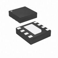
ATTINY9-MAHR Atmel, ATTINY9-MAHR Datasheet - Page 25

ATTINY9-MAHR
Manufacturer Part Number
ATTINY9-MAHR
Description
IC MCU AVR 1K FLASH 8UDFN
Manufacturer
Atmel
Series
AVR® ATtinyr
Datasheet
1.ATTINY9-MAHR.pdf
(169 pages)
Specifications of ATTINY9-MAHR
Package / Case
8-UDFN Exposed Pad
Voltage - Supply (vcc/vdd)
1.8 V ~ 5.5 V
Operating Temperature
-40°C ~ 85°C
Speed
12MHz
Number Of I /o
4
Core Processor
AVR
Program Memory Type
FLASH
Ram Size
32 x 8
Program Memory Size
1KB (1K x 8)
Oscillator Type
Internal
Peripherals
POR, PWM, WDT
Core Size
8-Bit
Lead Free Status / RoHS Status
Lead free / RoHS Compliant
Eeprom Size
-
Data Converters
-
Connectivity
-
Lead Free Status / Rohs Status
Details
Available stocks
Company
Part Number
Manufacturer
Quantity
Price
Company:
Part Number:
ATTINY9-MAHR
Manufacturer:
ST
Quantity:
101
- Current page: 25 of 169
- Download datasheet (5Mb)
7.3.1
7.3.2
7.3.3
7.3.4
7.4
7.4.1
8127D–AVR–02/10
Register Description
Analog Comparator
Analog to Digital Converter
Watchdog Timer
Port Pins
SMCR – Sleep Mode Control Register
When entering Idle mode, the analog comparator should be disabled if not used. In the power-
down mode, the analog comparator is automatically disabled. See
page 82
If enabled, the ADC will be enabled in all sleep modes. To save power, the ADC should be dis-
abled before entering any sleep mode. When the ADC is turned off and on again, the next
conversion will be an extended conversion. See
details on ADC operation.
The ADC is available in ATtiny5/10, only.
If the Watchdog Timer is not needed in the application, this module should be turned off. If the
Watchdog Timer is enabled, it will be enabled in all sleep modes, and hence, always consume
power. In the deeper sleep modes, this will contribute significantly to the total current consump-
tion. Refer to
When entering a sleep mode, all port pins should be configured to use minimum power. The
most important thing is then to ensure that no pins drive resistive loads. In sleep modes where
the I/O clock (clk
no power is consumed by the input logic when not needed. In some cases, the input logic is
needed for detecting wake-up conditions, and it will then be enabled. Refer to the section
Input Enable and Sleep Modes” on page 45
buffer is enabled and the input signal is left floating or has an analog signal level close to V
the input buffer will use excessive power.
For analog input pins, the digital input buffer should be disabled at all times. An analog signal
level close to V
input buffers can be disabled by writing to the Digital Input Disable Register (DIDR0). Refer to
“DIDR0 – Digital Input Disable Register 0” on page 83
The SMCR Control Register contains control bits for power management.
• Bits 7:4 – Res: Reserved Bits
These bits are reserved and will always read zero.
Bit
0x3A
Read/Write
Initial Value
for further details.
“Watchdog Timer” on page 30
CC
R
7
–
0
I/O
/2 on an input pin can cause significant current even in active mode. Digital
) is stopped, the input buffers of the device will be disabled. This ensures that
R
6
–
0
R
5
–
0
4
–
R
0
for details on how to configure the Watchdog Timer.
for details on which pins are enabled. If the input
SM2
R/W
3
0
“Analog to Digital Converter” on page 84
for details.
SM1
R/W
2
0
SM0
R/W
1
0
ATtiny4/5/9/10
“Analog Comparator” on
R/W
SE
0
0
SMCR
“Digital
CC
for
/2,
25
Related parts for ATTINY9-MAHR
Image
Part Number
Description
Manufacturer
Datasheet
Request
R

Part Number:
Description:
Manufacturer:
Atmel Corporation
Datasheet:

Part Number:
Description:
IC MCU AVR 1KB FLASH SOT-23-6
Manufacturer:
Atmel
Datasheet:

Part Number:
Description:
IC MCU AVR 1KB FLASH SOT-23-6
Manufacturer:
Atmel
Datasheet:

Part Number:
Description:
IC MCU AVR 1K FLASH 8UDFN
Manufacturer:
Atmel
Datasheet:

Part Number:
Description:
DEV KIT FOR AVR/AVR32
Manufacturer:
Atmel
Datasheet:

Part Number:
Description:
INTERVAL AND WIPE/WASH WIPER CONTROL IC WITH DELAY
Manufacturer:
ATMEL Corporation
Datasheet:

Part Number:
Description:
Low-Voltage Voice-Switched IC for Hands-Free Operation
Manufacturer:
ATMEL Corporation
Datasheet:

Part Number:
Description:
MONOLITHIC INTEGRATED FEATUREPHONE CIRCUIT
Manufacturer:
ATMEL Corporation
Datasheet:

Part Number:
Description:
AM-FM Receiver IC U4255BM-M
Manufacturer:
ATMEL Corporation
Datasheet:

Part Number:
Description:
Monolithic Integrated Feature Phone Circuit
Manufacturer:
ATMEL Corporation
Datasheet:

Part Number:
Description:
Multistandard Video-IF and Quasi Parallel Sound Processing
Manufacturer:
ATMEL Corporation
Datasheet:

Part Number:
Description:
High-performance EE PLD
Manufacturer:
ATMEL Corporation
Datasheet:


