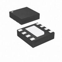
ATTINY9-MAHR Atmel, ATTINY9-MAHR Datasheet - Page 113

ATTINY9-MAHR
Manufacturer Part Number
ATTINY9-MAHR
Description
IC MCU AVR 1K FLASH 8UDFN
Manufacturer
Atmel
Series
AVR® ATtinyr
Datasheet
1.ATTINY9-MAHR.pdf
(169 pages)
Specifications of ATTINY9-MAHR
Package / Case
8-UDFN Exposed Pad
Voltage - Supply (vcc/vdd)
1.8 V ~ 5.5 V
Operating Temperature
-40°C ~ 85°C
Speed
12MHz
Number Of I /o
4
Core Processor
AVR
Program Memory Type
FLASH
Ram Size
32 x 8
Program Memory Size
1KB (1K x 8)
Oscillator Type
Internal
Peripherals
POR, PWM, WDT
Core Size
8-Bit
Lead Free Status / RoHS Status
Lead free / RoHS Compliant
Eeprom Size
-
Data Converters
-
Connectivity
-
Lead Free Status / Rohs Status
Details
Available stocks
Company
Part Number
Manufacturer
Quantity
Price
Company:
Part Number:
ATTINY9-MAHR
Manufacturer:
ST
Quantity:
101
- Current page: 113 of 169
- Download datasheet (5Mb)
15.4.2
15.4.3
15.4.3.1
8127D–AVR–02/10
Reading the Flash
Programming the Flash
Chip Erase
Figure 15-1. Addressing the Flash Memory
The Flash can be read from the data memory mapped locations one byte at a time. For read
operations, the least significant bit (bit 0) is used to select the low or high byte in the word
address. If this bit is zero, the low byte is read, and if it is one, the high byte is read.
The Flash can be written word-by-word. Before writing a Flash word, the Flash target location
must be erased. Writing to an un-erased Flash word will corrupt its content.
The Flash is word-accessed for writing, and the data space uses byte-addressing to access
Flash that has been mapped to data memory. It is therefore important to write the word in the
correct order to the Flash, namely low bytes before high bytes. First, the low byte is written to the
temporary buffer. Then, writing the high byte latches both the high byte and the low byte into the
Flash word buffer, starting the write operation to Flash.
The Flash erase operations can only performed for the entire Flash sections.
The Flash programming sequence is as follows:
The Chip Erase command will erase the entire code section of the Flash memory and the NVM
Lock Bits. For security reasons, the NVM Lock Bits are not reset before the code section has
been completely erased. Configuration, Signature and Calibration sections are not changed.
1. Perform a Flash section erase or perform a Chip erase
2. Write the Flash section word by word
ADDRESS POINTER
SECTIONEND
16
00
01
02
...
...
...
SECTION
FLASH
PAGE
PADDRMSB
WITHIN A FLASH
PAGE ADDRESS
SECTION
PADDR
PAGEEND
00
01
...
...
...
WADDRMSB+1
FLASH
WORD
PAGE
WADDRMSB
WADDR
ATtiny4/5/9/10
WORD ADDRESS
WITHIN A FLASH
PAGE
1
0/1
LOW/HIGH
BYTE SELECT
113
Related parts for ATTINY9-MAHR
Image
Part Number
Description
Manufacturer
Datasheet
Request
R

Part Number:
Description:
Manufacturer:
Atmel Corporation
Datasheet:

Part Number:
Description:
IC MCU AVR 1KB FLASH SOT-23-6
Manufacturer:
Atmel
Datasheet:

Part Number:
Description:
IC MCU AVR 1KB FLASH SOT-23-6
Manufacturer:
Atmel
Datasheet:

Part Number:
Description:
IC MCU AVR 1K FLASH 8UDFN
Manufacturer:
Atmel
Datasheet:

Part Number:
Description:
DEV KIT FOR AVR/AVR32
Manufacturer:
Atmel
Datasheet:

Part Number:
Description:
INTERVAL AND WIPE/WASH WIPER CONTROL IC WITH DELAY
Manufacturer:
ATMEL Corporation
Datasheet:

Part Number:
Description:
Low-Voltage Voice-Switched IC for Hands-Free Operation
Manufacturer:
ATMEL Corporation
Datasheet:

Part Number:
Description:
MONOLITHIC INTEGRATED FEATUREPHONE CIRCUIT
Manufacturer:
ATMEL Corporation
Datasheet:

Part Number:
Description:
AM-FM Receiver IC U4255BM-M
Manufacturer:
ATMEL Corporation
Datasheet:

Part Number:
Description:
Monolithic Integrated Feature Phone Circuit
Manufacturer:
ATMEL Corporation
Datasheet:

Part Number:
Description:
Multistandard Video-IF and Quasi Parallel Sound Processing
Manufacturer:
ATMEL Corporation
Datasheet:

Part Number:
Description:
High-performance EE PLD
Manufacturer:
ATMEL Corporation
Datasheet:


