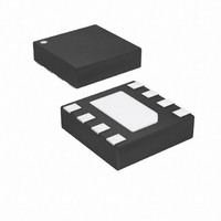
ATTINY9-MAHR Atmel, ATTINY9-MAHR Datasheet - Page 42

ATTINY9-MAHR
Manufacturer Part Number
ATTINY9-MAHR
Description
IC MCU AVR 1K FLASH 8UDFN
Manufacturer
Atmel
Series
AVR® ATtinyr
Datasheet
1.ATTINY9-MAHR.pdf
(169 pages)
Specifications of ATTINY9-MAHR
Package / Case
8-UDFN Exposed Pad
Voltage - Supply (vcc/vdd)
1.8 V ~ 5.5 V
Operating Temperature
-40°C ~ 85°C
Speed
12MHz
Number Of I /o
4
Core Processor
AVR
Program Memory Type
FLASH
Ram Size
32 x 8
Program Memory Size
1KB (1K x 8)
Oscillator Type
Internal
Peripherals
POR, PWM, WDT
Core Size
8-Bit
Lead Free Status / RoHS Status
Lead free / RoHS Compliant
Eeprom Size
-
Data Converters
-
Connectivity
-
Lead Free Status / Rohs Status
Details
Available stocks
Company
Part Number
Manufacturer
Quantity
Price
Company:
Part Number:
ATTINY9-MAHR
Manufacturer:
ST
Quantity:
101
- Current page: 42 of 169
- Download datasheet (5Mb)
10.2
10.2.1
42
Ports as General Digital I/O
ATtiny4/5/9/10
Configuring the Pin
The ports are bi-directional I/O ports with optional internal pull-ups.
tional description of one I/O-port pin, here generically called Pxn.
Figure 10-2. General Digital I/O
Note:
Each port pin consists of four register bits: DDxn, PORTxn, PUExn, and PINxn. As shown in
“Register Description” on page
PORTxn bits at the PORTx I/O address, the PUExn bits at the PUEx I/O address, and the PINxn
bits at the PINx I/O address.
Pxn
1. WEx, WRx, WPx, WDx, REx, RRx, RPx, and RDx are common to all pins within the same
port. clk
SLEEP:
clk
I/O
I/O
:
, and SLEEP are common to all ports.
SLEEP CONTROL
I/O CLOCK
SLEEP
51, the DDxn bits are accessed at the DDRx I/O address, the
(1)
SYNCHRONIZER
D
L
Q
Q
D
PINxn
Q
Q
RESET
RESET
RESET
PORTxn
WEx:
REx:
WDx:
RDx:
WRx:
RRx:
RPx:
WPx:
Q
Q
Q
Q
Q
Q
PUExn
DDxn
CLR
CLR
CLR
D
D
D
REx
RRx
WRITE PUEx
READ PUEx
WRITE DDRx
READ DDRx
WRITE PORTx
READ PORTx REGISTER
READ PORTx PIN
WRITE PINx REGISTER
Figure 10-2
WEx
WDx
RDx
RPx
clk
1
0
I/O
WRx
shows a func-
8127D–AVR–02/10
WPx
Related parts for ATTINY9-MAHR
Image
Part Number
Description
Manufacturer
Datasheet
Request
R

Part Number:
Description:
Manufacturer:
Atmel Corporation
Datasheet:

Part Number:
Description:
IC MCU AVR 1KB FLASH SOT-23-6
Manufacturer:
Atmel
Datasheet:

Part Number:
Description:
IC MCU AVR 1KB FLASH SOT-23-6
Manufacturer:
Atmel
Datasheet:

Part Number:
Description:
IC MCU AVR 1K FLASH 8UDFN
Manufacturer:
Atmel
Datasheet:

Part Number:
Description:
DEV KIT FOR AVR/AVR32
Manufacturer:
Atmel
Datasheet:

Part Number:
Description:
INTERVAL AND WIPE/WASH WIPER CONTROL IC WITH DELAY
Manufacturer:
ATMEL Corporation
Datasheet:

Part Number:
Description:
Low-Voltage Voice-Switched IC for Hands-Free Operation
Manufacturer:
ATMEL Corporation
Datasheet:

Part Number:
Description:
MONOLITHIC INTEGRATED FEATUREPHONE CIRCUIT
Manufacturer:
ATMEL Corporation
Datasheet:

Part Number:
Description:
AM-FM Receiver IC U4255BM-M
Manufacturer:
ATMEL Corporation
Datasheet:

Part Number:
Description:
Monolithic Integrated Feature Phone Circuit
Manufacturer:
ATMEL Corporation
Datasheet:

Part Number:
Description:
Multistandard Video-IF and Quasi Parallel Sound Processing
Manufacturer:
ATMEL Corporation
Datasheet:

Part Number:
Description:
High-performance EE PLD
Manufacturer:
ATMEL Corporation
Datasheet:


