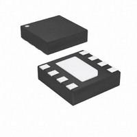
ATTINY9-MAHR Atmel, ATTINY9-MAHR Datasheet - Page 14

ATTINY9-MAHR
Manufacturer Part Number
ATTINY9-MAHR
Description
IC MCU AVR 1K FLASH 8UDFN
Manufacturer
Atmel
Series
AVR® ATtinyr
Datasheet
1.ATTINY9-MAHR.pdf
(169 pages)
Specifications of ATTINY9-MAHR
Package / Case
8-UDFN Exposed Pad
Voltage - Supply (vcc/vdd)
1.8 V ~ 5.5 V
Operating Temperature
-40°C ~ 85°C
Speed
12MHz
Number Of I /o
4
Core Processor
AVR
Program Memory Type
FLASH
Ram Size
32 x 8
Program Memory Size
1KB (1K x 8)
Oscillator Type
Internal
Peripherals
POR, PWM, WDT
Core Size
8-Bit
Lead Free Status / RoHS Status
Lead free / RoHS Compliant
Eeprom Size
-
Data Converters
-
Connectivity
-
Lead Free Status / Rohs Status
Details
Available stocks
Company
Part Number
Manufacturer
Quantity
Price
Company:
Part Number:
ATTINY9-MAHR
Manufacturer:
ST
Quantity:
101
- Current page: 14 of 169
- Download datasheet (5Mb)
5. Memories
5.1
5.2
14
In-System Re-programmable Flash Program Memory
Data Memory
ATtiny4/5/9/10
This section describes the different memories in the ATtiny4/5/9/10. Devices have two main
memory areas, the program memory space and the data memory space.
The ATtiny4/5/9/10 contain 512/1024 bytes of on-chip, in-system reprogrammable Flash mem-
ory for program storage. Since all AVR instructions are 16 or 32 bits wide, the Flash is organized
as 256/512 x 16.
The Flash memory has an endurance of at least 10,000 write/erase cycles. The ATtiny4/5/9/10
Program Counter (PC) is 9 bits wide, thus capable of addressing the 256/512 program memory
locations, starting at 0x000.
on Flash data serial downloading.
Constant tables can be allocated within the entire address space of program memory. Since pro-
gram memory can not be accessed directly, it has been mapped to the data memory. The
mapped program memory begins at byte address 0x4000 in data memory (see
page
must be addressed starting from 0x4000 when accessed via the data memory.
Internal write operations to Flash program memory have been disabled and program memory
therefore appears to firmware as read-only. Flash memory can still be written to externally but
internal write operations to the program memory area will not be succesful.
Timing diagrams of instruction fetch and execution are presented in
ing” on page
Data memory locations include the I/O memory, the internal SRAM memory, the non-volatile
memory lock bits, and the Flash memory. See
the ATtiny4/5/9/10 memory space is organized.
The first 64 locations are reserved for I/O memory, while the following 32 data memory locations
address the internal data SRAM.
The non-volatile memory lock bits and all the Flash memory sections are mapped to the data
memory space. These locations appear as read-only for device firmware.
The four different addressing modes for data memory are direct, indirect, indirect with pre-decre-
ment, and indirect with post-increment. In the register file, registers R26 to R31 function as
pointer registers for indirect addressing.
The IN and OUT instructions can access all 64 locations of I/O memory. Direct addressing using
the LDS and STS instructions reaches the 128 locations between 0x0040 and 0x00BF.
The indirect addressing reaches the entire data memory space. When using indirect addressing
modes with automatic pre-decrement and post-increment, the address registers X, Y, and Z are
decremented or incremented.
15). Although programs are executed starting from address 0x000 in program memory it
9.
“Memory Programming” on page 108
Figure 5-1 on page 15
contains a detailed description
“Instruction Execution Tim-
for an illustration on how
Figure 5-1 on
8127D–AVR–02/10
Related parts for ATTINY9-MAHR
Image
Part Number
Description
Manufacturer
Datasheet
Request
R

Part Number:
Description:
Manufacturer:
Atmel Corporation
Datasheet:

Part Number:
Description:
IC MCU AVR 1KB FLASH SOT-23-6
Manufacturer:
Atmel
Datasheet:

Part Number:
Description:
IC MCU AVR 1KB FLASH SOT-23-6
Manufacturer:
Atmel
Datasheet:

Part Number:
Description:
IC MCU AVR 1K FLASH 8UDFN
Manufacturer:
Atmel
Datasheet:

Part Number:
Description:
DEV KIT FOR AVR/AVR32
Manufacturer:
Atmel
Datasheet:

Part Number:
Description:
INTERVAL AND WIPE/WASH WIPER CONTROL IC WITH DELAY
Manufacturer:
ATMEL Corporation
Datasheet:

Part Number:
Description:
Low-Voltage Voice-Switched IC for Hands-Free Operation
Manufacturer:
ATMEL Corporation
Datasheet:

Part Number:
Description:
MONOLITHIC INTEGRATED FEATUREPHONE CIRCUIT
Manufacturer:
ATMEL Corporation
Datasheet:

Part Number:
Description:
AM-FM Receiver IC U4255BM-M
Manufacturer:
ATMEL Corporation
Datasheet:

Part Number:
Description:
Monolithic Integrated Feature Phone Circuit
Manufacturer:
ATMEL Corporation
Datasheet:

Part Number:
Description:
Multistandard Video-IF and Quasi Parallel Sound Processing
Manufacturer:
ATMEL Corporation
Datasheet:

Part Number:
Description:
High-performance EE PLD
Manufacturer:
ATMEL Corporation
Datasheet:


