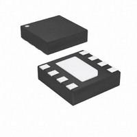
ATTINY9-MAHR Atmel, ATTINY9-MAHR Datasheet - Page 50

ATTINY9-MAHR
Manufacturer Part Number
ATTINY9-MAHR
Description
IC MCU AVR 1K FLASH 8UDFN
Manufacturer
Atmel
Series
AVR® ATtinyr
Datasheet
1.ATTINY9-MAHR.pdf
(169 pages)
Specifications of ATTINY9-MAHR
Package / Case
8-UDFN Exposed Pad
Voltage - Supply (vcc/vdd)
1.8 V ~ 5.5 V
Operating Temperature
-40°C ~ 85°C
Speed
12MHz
Number Of I /o
4
Core Processor
AVR
Program Memory Type
FLASH
Ram Size
32 x 8
Program Memory Size
1KB (1K x 8)
Oscillator Type
Internal
Peripherals
POR, PWM, WDT
Core Size
8-Bit
Lead Free Status / RoHS Status
Lead free / RoHS Compliant
Eeprom Size
-
Data Converters
-
Connectivity
-
Lead Free Status / Rohs Status
Details
Available stocks
Company
Part Number
Manufacturer
Quantity
Price
Company:
Part Number:
ATTINY9-MAHR
Manufacturer:
ST
Quantity:
101
- Current page: 50 of 169
- Download datasheet (5Mb)
50
ATtiny4/5/9/10
• Port B, Bit 2 – ADC2/CLKO/INT0/PCINT2/T0
• Port B, Bit 3 – ADC3/PCINT3/RESET
Table 10-4
signals shown in
Table 10-4.
Notes:
Signal
Name
PUOE
PUOV
DDOE
DDOV
PVOE
PVOV
PTOE
DIEOE
DIEOV
DI
AIO
• OC0B: Output Compare Match output: The PB1 pin can serve as an external output for the
• PCINT1: Pin Change Interrupt source 1. The PB1 pin can serve as an external interrupt
• TPICLK: Serial Programming Clock.
• ADC2: Analog to Digital Converter, Channel 2
• CLKO: System Clock Output. The system clock can be output on pin PB2. The system clock
• INT0: External Interrupt Request 0
• PCINT2: Pin Change Interrupt source 2. The PB2 pin can serve as an external interrupt
• T0: Timer/Counter0 counter source.
• ADC3: Analog to Digital Converter, Channel 3
• PCINT3: Pin Change Interrupt source 3. The PB3 pin can serve as an external interrupt
• RESET:
Timer/Counter0 Compare Match B. The PB1 pin has to be configured as an output (DDB1
set (one)) to serve this function. The OC0B pin is also the output pin for the PWM mode timer
function.
source for pin change interrupt 0.
will be output if CKOUT bit is programmed, regardless of the PORTB2 and DDB2 settings.
source for pin change interrupt 0.
source for pin change interrupt 0.
1. RSTDISBL is 1 when the configuration bit is “0” (Programmed).
2. CKOUT is 1 when the configuration bit is “0” (Programmed).
and
Overriding Signals for Alternate Functions in PB3..PB2
PB3/ADC3/RESET/PCINT3
RSTDISBL
1
RSTDISBL
0
0
0
0
RSTDISBL
ADC3D
RSTDISBL • PCINT3 • PCIE0
PCINT3 Input
ADC3 Input
Table 10-5 on page 51
Figure 10-6 on page
(1)
(1)
(1)
+ (PCINT3 • PCIE0) +
47.
relate the alternate functions of Port B to the overriding
(ATtiny5/10, only)
(ATtiny5/10, only)
PB2/ADC2/INT0/T0/CLKO/PCINT2
CKOUT
0
CKOUT
1
CKOUT
(system clock)
0
(PCINT2 • PCIE0) + ADC2D + INT0
(PCINT2 • PCIE0) + INT0
INT0/T0/PCINT2 Input
ADC2 Input
(2)
(2)
(2)
8127D–AVR–02/10
Related parts for ATTINY9-MAHR
Image
Part Number
Description
Manufacturer
Datasheet
Request
R

Part Number:
Description:
Manufacturer:
Atmel Corporation
Datasheet:

Part Number:
Description:
IC MCU AVR 1KB FLASH SOT-23-6
Manufacturer:
Atmel
Datasheet:

Part Number:
Description:
IC MCU AVR 1KB FLASH SOT-23-6
Manufacturer:
Atmel
Datasheet:

Part Number:
Description:
IC MCU AVR 1K FLASH 8UDFN
Manufacturer:
Atmel
Datasheet:

Part Number:
Description:
DEV KIT FOR AVR/AVR32
Manufacturer:
Atmel
Datasheet:

Part Number:
Description:
INTERVAL AND WIPE/WASH WIPER CONTROL IC WITH DELAY
Manufacturer:
ATMEL Corporation
Datasheet:

Part Number:
Description:
Low-Voltage Voice-Switched IC for Hands-Free Operation
Manufacturer:
ATMEL Corporation
Datasheet:

Part Number:
Description:
MONOLITHIC INTEGRATED FEATUREPHONE CIRCUIT
Manufacturer:
ATMEL Corporation
Datasheet:

Part Number:
Description:
AM-FM Receiver IC U4255BM-M
Manufacturer:
ATMEL Corporation
Datasheet:

Part Number:
Description:
Monolithic Integrated Feature Phone Circuit
Manufacturer:
ATMEL Corporation
Datasheet:

Part Number:
Description:
Multistandard Video-IF and Quasi Parallel Sound Processing
Manufacturer:
ATMEL Corporation
Datasheet:

Part Number:
Description:
High-performance EE PLD
Manufacturer:
ATMEL Corporation
Datasheet:


