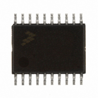
MC9S08EL16CTJ Freescale Semiconductor, MC9S08EL16CTJ Datasheet - Page 80

MC9S08EL16CTJ
Manufacturer Part Number
MC9S08EL16CTJ
Description
MCU 16KB FLASH SLIC 20TSSOP
Manufacturer
Freescale Semiconductor
Series
HCS08r
Datasheet
1.DEMO9S08EL32.pdf
(356 pages)
Specifications of MC9S08EL16CTJ
Core Processor
HCS08
Core Size
8-Bit
Speed
40MHz
Connectivity
I²C, LIN, SCI, SPI
Peripherals
LVD, POR, PWM, WDT
Number Of I /o
16
Program Memory Size
16KB (16K x 8)
Program Memory Type
FLASH
Eeprom Size
512 x 8
Ram Size
1K x 8
Voltage - Supply (vcc/vdd)
2.7 V ~ 5.5 V
Data Converters
A/D 12x10b
Oscillator Type
External
Operating Temperature
-40°C ~ 85°C
Package / Case
20-TSSOP
Processor Series
S08EL
Core
HCS08
Data Bus Width
8 bit
Data Ram Size
1 KB
Interface Type
SCI, SPI, I2C, SLIC
Maximum Clock Frequency
200 KHz
Number Of Programmable I/os
16
Number Of Timers
2
Operating Supply Voltage
5.5 V
Maximum Operating Temperature
+ 85 C
Mounting Style
SMD/SMT
3rd Party Development Tools
EWS08
Development Tools By Supplier
DEMO9S08EL32AUTO, DEMO9S08EL32
Minimum Operating Temperature
- 40 C
On-chip Adc
10 bit, 12 Channel
For Use With
DEMO9S08EL32 - BOARD DEMO FOR 9S08 EL MCUDEMO9S08EL32AUTO - DEMO BOARD EL32 AUTO
Lead Free Status / RoHS Status
Lead free / RoHS Compliant
- Current page: 80 of 356
- Download datasheet (9Mb)
Chapter 6 Parallel Input/Output Control
It is a good programming practice to write to the port data register before changing the direction of a port
pin to become an output. This ensures that the pin will not be driven momentarily with an old data value
that happened to be in the port data register.
6.2
Associated with the parallel I/O ports is a set of registers located in the high page register space that operate
independently of the parallel I/O registers. These registers are used to control pull-ups, slew rate, and drive
strength for the pins.
An internal pull-up device can be enabled for each port pin by setting the corresponding bit in the pull-up
enable register (PTxPEn). The pull-up device is disabled if the pin is configured as an output by the parallel
I/O control logic or any shared peripheral function regardless of the state of the corresponding pull-up
enable register bit. The pull-up device is also disabled if the pin is controlled by an analog function.
Slew rate control can be enabled for each port pin by setting the corresponding bit in the slew rate control
register (PTxSEn). When enabled, slew control limits the rate at which an output can transition in order to
reduce EMC emissions. Slew rate control has no effect on pins that are configured as inputs.
An output pin can be selected to have high output drive strength by setting the corresponding bit in the
drive strength select register (PTxDSn). When high drive is selected, a pin is capable of sourcing and
sinking greater current. Even though every I/O pin can be selected as high drive, the user must ensure that
the total current source and sink limits for the MCU are not exceeded. Drive strength selection is intended
to affect the DC behavior of I/O pins. However, the AC behavior is also affected. High drive allows a pin
to drive a greater load with the same switching speed as a low drive enabled pin into a smaller load.
Because of this, the EMC emissions may be affected by enabling pins as high drive.
80
Pull-up, Slew Rate, and Drive Strength
Port Read
BUSCLK
Data
MC9S08EL32 Series and MC9S08SL16 Series Data Sheet, Rev. 3
Figure 6-1. Parallel I/O Block Diagram
PTxDDn
D
D
PTxDn
Q
Q
1
0
Synchronizer
Output Enable
Output Data
Freescale Semiconductor
Input Data
Related parts for MC9S08EL16CTJ
Image
Part Number
Description
Manufacturer
Datasheet
Request
R
Part Number:
Description:
Manufacturer:
Freescale Semiconductor, Inc
Datasheet:
Part Number:
Description:
Manufacturer:
Freescale Semiconductor, Inc
Datasheet:
Part Number:
Description:
Manufacturer:
Freescale Semiconductor, Inc
Datasheet:
Part Number:
Description:
Manufacturer:
Freescale Semiconductor, Inc
Datasheet:
Part Number:
Description:
Manufacturer:
Freescale Semiconductor, Inc
Datasheet:
Part Number:
Description:
Manufacturer:
Freescale Semiconductor, Inc
Datasheet:
Part Number:
Description:
Manufacturer:
Freescale Semiconductor, Inc
Datasheet:
Part Number:
Description:
Manufacturer:
Freescale Semiconductor, Inc
Datasheet:
Part Number:
Description:
Manufacturer:
Freescale Semiconductor, Inc
Datasheet:
Part Number:
Description:
Manufacturer:
Freescale Semiconductor, Inc
Datasheet:
Part Number:
Description:
Manufacturer:
Freescale Semiconductor, Inc
Datasheet:
Part Number:
Description:
Manufacturer:
Freescale Semiconductor, Inc
Datasheet:
Part Number:
Description:
Manufacturer:
Freescale Semiconductor, Inc
Datasheet:
Part Number:
Description:
Manufacturer:
Freescale Semiconductor, Inc
Datasheet:
Part Number:
Description:
Manufacturer:
Freescale Semiconductor, Inc
Datasheet:


