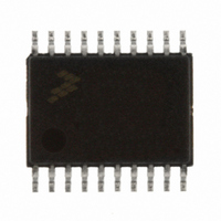
MC9S08EL16CTJ Freescale Semiconductor, MC9S08EL16CTJ Datasheet - Page 103

MC9S08EL16CTJ
Manufacturer Part Number
MC9S08EL16CTJ
Description
MCU 16KB FLASH SLIC 20TSSOP
Manufacturer
Freescale Semiconductor
Series
HCS08r
Datasheet
1.DEMO9S08EL32.pdf
(356 pages)
Specifications of MC9S08EL16CTJ
Core Processor
HCS08
Core Size
8-Bit
Speed
40MHz
Connectivity
I²C, LIN, SCI, SPI
Peripherals
LVD, POR, PWM, WDT
Number Of I /o
16
Program Memory Size
16KB (16K x 8)
Program Memory Type
FLASH
Eeprom Size
512 x 8
Ram Size
1K x 8
Voltage - Supply (vcc/vdd)
2.7 V ~ 5.5 V
Data Converters
A/D 12x10b
Oscillator Type
External
Operating Temperature
-40°C ~ 85°C
Package / Case
20-TSSOP
Processor Series
S08EL
Core
HCS08
Data Bus Width
8 bit
Data Ram Size
1 KB
Interface Type
SCI, SPI, I2C, SLIC
Maximum Clock Frequency
200 KHz
Number Of Programmable I/os
16
Number Of Timers
2
Operating Supply Voltage
5.5 V
Maximum Operating Temperature
+ 85 C
Mounting Style
SMD/SMT
3rd Party Development Tools
EWS08
Development Tools By Supplier
DEMO9S08EL32AUTO, DEMO9S08EL32
Minimum Operating Temperature
- 40 C
On-chip Adc
10 bit, 12 Channel
For Use With
DEMO9S08EL32 - BOARD DEMO FOR 9S08 EL MCUDEMO9S08EL32AUTO - DEMO BOARD EL32 AUTO
Lead Free Status / RoHS Status
Lead free / RoHS Compliant
- Current page: 103 of 356
- Download datasheet (9Mb)
7.4.5
The BGND instruction is new to the HCS08 compared to the M68HC08. BGND would not be used in
normal user programs because it forces the CPU to stop processing user instructions and enter the active
background mode. The only way to resume execution of the user program is through reset or by a host
debug system issuing a GO, TRACE1, or TAGGO serial command through the background debug
interface.
Software-based breakpoints can be set by replacing an opcode at the desired breakpoint address with the
BGND opcode. When the program reaches this breakpoint address, the CPU is forced to active
background mode rather than continuing the user program.
7.5
Table 7-2
shows operand construction, execution time in internal bus clock cycles, and cycle-by-cycle details for
each addressing mode variation of each instruction.
Freescale Semiconductor
ADC #opr8i
ADC opr8a
ADC opr16a
ADC oprx16,X
ADC oprx8,X
ADC ,X
ADC oprx16,SP
ADC oprx8,SP
ADD #opr8i
ADD opr8a
ADD opr16a
ADD oprx16,X
ADD oprx8,X
ADD ,X
ADD oprx16,SP
ADD oprx8,SP
AIS #opr8i
AIX #opr8i
AND #opr8i
AND opr8a
AND opr16a
AND oprx16,X
AND oprx8,X
AND ,X
AND oprx16,SP
AND oprx8,SP
Source
Form
HCS08 Instruction Set Summary
provides a summary of the HCS08 instruction set in all possible addressing modes. The table
BGND Instruction
Add with Carry
A ← (A) + (M) + (C)
Add without Carry
A ← (A) + (M)
Add Immediate Value (Signed) to
Stack Pointer
SP ← (SP) + (M)
Add Immediate Value (Signed) to
Index Register (H:X)
H:X ← (H:X) + (M)
Logical AND
A ← (A) & (M)
MC9S08EL32 Series and MC9S08SL16 Series Data Sheet, Rev. 3
Table 7-2. Instruction Set Summary (Sheet 1 of 9)
Operation
IMM
DIR
EXT
IX2
IX1
IX
SP2
SP1
IMM
DIR
EXT
IX2
IX1
IX
SP2
SP1
IMM
IMM
IMM
DIR
EXT
IX2
IX1
IX
SP2
SP1
Object Code
9E D9
9E E9
9E DB
9E EB
9E D4
9E E4
A9
B9
C9
D9
E9
F9
AB
BB
CB
DB
EB
FB
A7 ii
AF ii
A4
B4
C4
D4
E4
F4
ii
dd
hh ll
ee ff
ff
ee ff
ff
ii
dd
hh ll
ee ff
ff
ee ff
ff
ii
dd
hh ll
ee ff
ff
ee ff
ff
Chapter 7 Central Processor Unit (S08CPUV3)
2
3
4
4
3
3
5
4
2
3
4
4
3
3
5
4
2
2
2
3
4
4
3
3
5
4
pp
rpp
prpp
prpp
rpp
rfp
pprpp
prpp
pp
rpp
prpp
prpp
rpp
rfp
pprpp
prpp
pp
pp
pp
rpp
prpp
prpp
rpp
rfp
pprpp
prpp
Cyc-by-Cyc
Details
V 1 1 H I N Z C
– 1 1 – – – – –
– 1 1 – – – – –
0 1 1 – –
1 1
1 1
on CCR
Affect
–
–
103
–
Related parts for MC9S08EL16CTJ
Image
Part Number
Description
Manufacturer
Datasheet
Request
R
Part Number:
Description:
Manufacturer:
Freescale Semiconductor, Inc
Datasheet:
Part Number:
Description:
Manufacturer:
Freescale Semiconductor, Inc
Datasheet:
Part Number:
Description:
Manufacturer:
Freescale Semiconductor, Inc
Datasheet:
Part Number:
Description:
Manufacturer:
Freescale Semiconductor, Inc
Datasheet:
Part Number:
Description:
Manufacturer:
Freescale Semiconductor, Inc
Datasheet:
Part Number:
Description:
Manufacturer:
Freescale Semiconductor, Inc
Datasheet:
Part Number:
Description:
Manufacturer:
Freescale Semiconductor, Inc
Datasheet:
Part Number:
Description:
Manufacturer:
Freescale Semiconductor, Inc
Datasheet:
Part Number:
Description:
Manufacturer:
Freescale Semiconductor, Inc
Datasheet:
Part Number:
Description:
Manufacturer:
Freescale Semiconductor, Inc
Datasheet:
Part Number:
Description:
Manufacturer:
Freescale Semiconductor, Inc
Datasheet:
Part Number:
Description:
Manufacturer:
Freescale Semiconductor, Inc
Datasheet:
Part Number:
Description:
Manufacturer:
Freescale Semiconductor, Inc
Datasheet:
Part Number:
Description:
Manufacturer:
Freescale Semiconductor, Inc
Datasheet:
Part Number:
Description:
Manufacturer:
Freescale Semiconductor, Inc
Datasheet:


