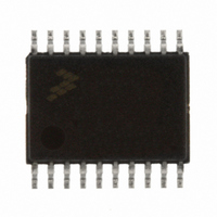
MC9S08EL16CTJ Freescale Semiconductor, MC9S08EL16CTJ Datasheet - Page 145

MC9S08EL16CTJ
Manufacturer Part Number
MC9S08EL16CTJ
Description
MCU 16KB FLASH SLIC 20TSSOP
Manufacturer
Freescale Semiconductor
Series
HCS08r
Datasheet
1.DEMO9S08EL32.pdf
(356 pages)
Specifications of MC9S08EL16CTJ
Core Processor
HCS08
Core Size
8-Bit
Speed
40MHz
Connectivity
I²C, LIN, SCI, SPI
Peripherals
LVD, POR, PWM, WDT
Number Of I /o
16
Program Memory Size
16KB (16K x 8)
Program Memory Type
FLASH
Eeprom Size
512 x 8
Ram Size
1K x 8
Voltage - Supply (vcc/vdd)
2.7 V ~ 5.5 V
Data Converters
A/D 12x10b
Oscillator Type
External
Operating Temperature
-40°C ~ 85°C
Package / Case
20-TSSOP
Processor Series
S08EL
Core
HCS08
Data Bus Width
8 bit
Data Ram Size
1 KB
Interface Type
SCI, SPI, I2C, SLIC
Maximum Clock Frequency
200 KHz
Number Of Programmable I/os
16
Number Of Timers
2
Operating Supply Voltage
5.5 V
Maximum Operating Temperature
+ 85 C
Mounting Style
SMD/SMT
3rd Party Development Tools
EWS08
Development Tools By Supplier
DEMO9S08EL32AUTO, DEMO9S08EL32
Minimum Operating Temperature
- 40 C
On-chip Adc
10 bit, 12 Channel
For Use With
DEMO9S08EL32 - BOARD DEMO FOR 9S08 EL MCUDEMO9S08EL32AUTO - DEMO BOARD EL32 AUTO
Lead Free Status / RoHS Status
Lead free / RoHS Compliant
- Current page: 145 of 356
- Download datasheet (9Mb)
10.3.2
The ADCSC2 register is used to control the compare function, conversion trigger and conversion active
of the ADC module.
Freescale Semiconductor
ADTRG
ADACT
Field
1
7
6
Bits 1 and 0 are reserved bits that must always be written to 0.
Reset:
W
R
Status and Control Register 2 (ADCSC2)
Conversion Active — ADACT indicates that a conversion is in progress. ADACT is set when a conversion is
initiated and cleared when a conversion is completed or aborted.
0 Conversion not in progress
1 Conversion in progress
Conversion Trigger Select — ADTRG is used to select the type of trigger to be used for initiating a conversion.
Two types of trigger are selectable: software trigger and hardware trigger. When software trigger is selected, a
conversion is initiated following a write to ADCSC1. When hardware trigger is selected, a conversion is initiated
following the assertion of the ADHWT input.
0 Software trigger selected
1 Hardware trigger selected
ADACT
7
0
ADCH
01000
01001
01010
01011
01100
01101
01110
01111
MC9S08EL32 Series and MC9S08SL16 Series Data Sheet, Rev. 3
= Unimplemented or Reserved
ADTRG
Figure 10-5. Status and Control Register 2 (ADCSC2)
Table 10-4. ADCSC2 Register Field Descriptions
0
6
Figure 10-4. Input Channel Select (continued)
Input Select
ACFE
0
5
AD10
AD11
AD12
AD13
AD14
AD15
AD8
AD9
ACFGT
0
4
Description
0
0
3
Analog-to-Digital Converter (S08ADC10V1)
ADCH
11000
11001
11010
11011
11100
11101
11110
11111
0
0
2
R
0
1
1
Module disabled
Input Select
Reserved
V
V
AD24
AD25
AD26
AD27
REFH
REFL
R
0
0
1
145
Related parts for MC9S08EL16CTJ
Image
Part Number
Description
Manufacturer
Datasheet
Request
R
Part Number:
Description:
Manufacturer:
Freescale Semiconductor, Inc
Datasheet:
Part Number:
Description:
Manufacturer:
Freescale Semiconductor, Inc
Datasheet:
Part Number:
Description:
Manufacturer:
Freescale Semiconductor, Inc
Datasheet:
Part Number:
Description:
Manufacturer:
Freescale Semiconductor, Inc
Datasheet:
Part Number:
Description:
Manufacturer:
Freescale Semiconductor, Inc
Datasheet:
Part Number:
Description:
Manufacturer:
Freescale Semiconductor, Inc
Datasheet:
Part Number:
Description:
Manufacturer:
Freescale Semiconductor, Inc
Datasheet:
Part Number:
Description:
Manufacturer:
Freescale Semiconductor, Inc
Datasheet:
Part Number:
Description:
Manufacturer:
Freescale Semiconductor, Inc
Datasheet:
Part Number:
Description:
Manufacturer:
Freescale Semiconductor, Inc
Datasheet:
Part Number:
Description:
Manufacturer:
Freescale Semiconductor, Inc
Datasheet:
Part Number:
Description:
Manufacturer:
Freescale Semiconductor, Inc
Datasheet:
Part Number:
Description:
Manufacturer:
Freescale Semiconductor, Inc
Datasheet:
Part Number:
Description:
Manufacturer:
Freescale Semiconductor, Inc
Datasheet:
Part Number:
Description:
Manufacturer:
Freescale Semiconductor, Inc
Datasheet:


