MC9S08EL16CTJ Freescale Semiconductor, MC9S08EL16CTJ Datasheet - Page 3
MC9S08EL16CTJ
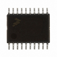
Manufacturer Part Number
MC9S08EL16CTJ
Description
MCU 16KB FLASH SLIC 20TSSOP
Manufacturer
Freescale Semiconductor
Series
HCS08r
Datasheet
1.DEMO9S08EL32.pdf
(356 pages)
Specifications of MC9S08EL16CTJ
Core Processor
HCS08
Core Size
8-Bit
Speed
40MHz
Connectivity
I²C, LIN, SCI, SPI
Peripherals
LVD, POR, PWM, WDT
Number Of I /o
16
Program Memory Size
16KB (16K x 8)
Program Memory Type
FLASH
Eeprom Size
512 x 8
Ram Size
1K x 8
Voltage - Supply (vcc/vdd)
2.7 V ~ 5.5 V
Data Converters
A/D 12x10b
Oscillator Type
External
Operating Temperature
-40°C ~ 85°C
Package / Case
20-TSSOP
Processor Series
S08EL
Core
HCS08
Data Bus Width
8 bit
Data Ram Size
1 KB
Interface Type
SCI, SPI, I2C, SLIC
Maximum Clock Frequency
200 KHz
Number Of Programmable I/os
16
Number Of Timers
2
Operating Supply Voltage
5.5 V
Maximum Operating Temperature
+ 85 C
Mounting Style
SMD/SMT
3rd Party Development Tools
EWS08
Development Tools By Supplier
DEMO9S08EL32AUTO, DEMO9S08EL32
Minimum Operating Temperature
- 40 C
On-chip Adc
10 bit, 12 Channel
For Use With
DEMO9S08EL32 - BOARD DEMO FOR 9S08 EL MCUDEMO9S08EL32AUTO - DEMO BOARD EL32 AUTO
Lead Free Status / RoHS Status
Lead free / RoHS Compliant


MC9S08EL32 Features
8-Bit HCS08 Central Processor Unit (CPU)
On-Chip Memory
Power-Saving Modes
Clock Source Options
System Protection
Development Support
• 40-MHz HCS08 CPU (central processor unit)
• HC08 instruction set with added BGND instruction
• Support for up to 32 interrupt/reset sources
• FLASH read/program/erase over full operating
• EEPROM in-circuit programmable memory;
• Random-access memory (RAM)
• Security circuitry to prevent unauthorized access
• Two very low-power stop modes
• Reduced power wait mode
• Very low-power real-time interrupt for use in run,
• Oscillator (XOSC) — Loop-control Pierce
• Internal clock source (ICS) — Contains a
• Watchdog computer operating properly (COP)
• Low-voltage detection with reset or interrupt;
• Illegal opcode detection with reset
• Illegal address detection with reset
• FLASH and EEPROM block protect
• Single-wire background debug interface
• Breakpoint capability allows single breakpoint
• In-circuit emulation (ICE) debug module —
voltage and temperature
program and erase while executing FLASH; erase
abort
to RAM and NVM contents
wait, and stop
oscillator; Crystal or ceramic resonator range of
31.25 kHz to 38.4 kHz or 1 MHz to 16 MHz
frequency-locked loop (FLL) controlled by internal
or external reference; precision trimming of
internal reference allows 0.2% resolution and 2%
deviation over temperature and voltage; supports
bus frequencies from 2–20 MHz
reset with option to run from dedicated 1-kHz
internal clock source or bus clock
selectable trip points
setting during in-circuit debugging (plus two more
breakpoints in the on-chip debug module)
contains two comparators and nine trigger modes;
eight-deep FIFO for storing change-of-flow
address and event-only data; supports both tag
and force breakpoints
Peripherals
Input/Output
Package Options
• ADC — 16-channel, 10-bit resolution, 2.5 μs
• ACMPx — Two analog comparators with
• SCI — Full duplex non-return to zero (NRZ); LIN
• SLIC — Supports LIN 2.0 and SAE J2602
• SPI — Full-duplex or single-wire bidirectional;
• IIC — Up to 100 kbps with maximum bus loading;
• TPMx — One 4-channel (TPM1) and one
• RTC — 8-bit modulus real-time counter with
• 22 general purpose I/O pins
• 16 interrupt pins with selectable polarity
• Hysteresis and configurable pull up device on all
• 28-TSSOP
• 20-TSSOP
conversion time, automatic compare function,
temperature sensor, internal bandgap reference
channel; runs in stop3
selectable interrupt on rising, falling, or either
edge of comparator output; compare option to
fixed internal bandgap reference voltage; output
can optionally be routed to TPM module; runs in
stop3
master extended break generation; LIN slave
extended break detection; wake-up on active
edge
protocols; up to 120 kbps, full LIN message
buffering, automatic bit rate and frame
synchronization, checksum generation and
verification, UART-like byte transfer mode
double-buffered transmit and receive; master or
slave mode; MSB-first or LSB-first shifting
Multi-master operation; Programmable slave
address; Interrupt driven byte-by-byte data
transfer
2-channel (TPM2); selectable input capture,
output compare, or buffered edge- or
center-aligned PWM on each channel
binary or decimal based prescaler; external clock
source for precise time base, time-of-day,
calendar, or task scheduling functions; free
running on-chip low power oscillator (1 kHz) for
cyclic wake-up without external components
input pins; Configurable slew rate and drive
strength on all output pins.
Related parts for MC9S08EL16CTJ
Image
Part Number
Description
Manufacturer
Datasheet
Request
R

Part Number:
Description:
Manufacturer:
Freescale Semiconductor, Inc
Datasheet:
Part Number:
Description:
Manufacturer:
Freescale Semiconductor, Inc
Datasheet:
Part Number:
Description:
Manufacturer:
Freescale Semiconductor, Inc
Datasheet:
Part Number:
Description:
Manufacturer:
Freescale Semiconductor, Inc
Datasheet:
Part Number:
Description:
Manufacturer:
Freescale Semiconductor, Inc
Datasheet:
Part Number:
Description:
Manufacturer:
Freescale Semiconductor, Inc
Datasheet:
Part Number:
Description:
Manufacturer:
Freescale Semiconductor, Inc
Datasheet:
Part Number:
Description:
Manufacturer:
Freescale Semiconductor, Inc
Datasheet:
Part Number:
Description:
Manufacturer:
Freescale Semiconductor, Inc
Datasheet:
Part Number:
Description:
Manufacturer:
Freescale Semiconductor, Inc
Datasheet:
Part Number:
Description:
Manufacturer:
Freescale Semiconductor, Inc
Datasheet:
Part Number:
Description:
Manufacturer:
Freescale Semiconductor, Inc
Datasheet:
Part Number:
Description:
Manufacturer:
Freescale Semiconductor, Inc
Datasheet:
Part Number:
Description:
Manufacturer:
Freescale Semiconductor, Inc
Datasheet:
Part Number:
Description:
Manufacturer:
Freescale Semiconductor, Inc
Datasheet: