MC9S08EL16CTJ Freescale Semiconductor, MC9S08EL16CTJ Datasheet - Page 234
MC9S08EL16CTJ
Manufacturer Part Number
MC9S08EL16CTJ
Description
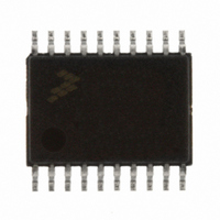
MCU 16KB FLASH SLIC 20TSSOP
Manufacturer
Freescale Semiconductor
Series
HCS08r
Datasheet
1.DEMO9S08EL32.pdf
(356 pages)
Specifications of MC9S08EL16CTJ
Core Processor
HCS08
Core Size
8-Bit
Speed
40MHz
Connectivity
I²C, LIN, SCI, SPI
Peripherals
LVD, POR, PWM, WDT
Number Of I /o
16
Program Memory Size
16KB (16K x 8)
Program Memory Type
FLASH
Eeprom Size
512 x 8
Ram Size
1K x 8
Voltage - Supply (vcc/vdd)
2.7 V ~ 5.5 V
Data Converters
A/D 12x10b
Oscillator Type
External
Operating Temperature
-40°C ~ 85°C
Package / Case
20-TSSOP
Processor Series
S08EL
Core
HCS08
Data Bus Width
8 bit
Data Ram Size
1 KB
Interface Type
SCI, SPI, I2C, SLIC
Maximum Clock Frequency
200 KHz
Number Of Programmable I/os
16
Number Of Timers
2
Operating Supply Voltage
5.5 V
Maximum Operating Temperature
+ 85 C
Mounting Style
SMD/SMT
3rd Party Development Tools
EWS08
Development Tools By Supplier
DEMO9S08EL32AUTO, DEMO9S08EL32
Minimum Operating Temperature
- 40 C
On-chip Adc
10 bit, 12 Channel
For Use With
DEMO9S08EL32 - BOARD DEMO FOR 9S08 EL MCUDEMO9S08EL32AUTO - DEMO BOARD EL32 AUTO
Lead Free Status / RoHS Status
Lead free / RoHS Compliant


Serial Peripheral Interface (S08SPIV3)
The most common uses of the SPI system include connecting simple shift registers for adding input or
output ports or connecting small peripheral devices such as serial A/D or D/A converters. Although
Figure 13-2
simpler connections where data is unidirectionally transferred from the master MCU to a slave or from a
slave to the master MCU.
13.1.2.2
Figure 13-3
Data is written to the double-buffered transmitter (write to SPID) and gets transferred to the SPI shift
register at the start of a data transfer. After shifting in a byte of data, the data is transferred into the
double-buffered receiver where it can be read (read from SPID). Pin multiplexing logic controls
connections between MCU pins and the SPI module.
When the SPI is configured as a master, the clock output is routed to the SPSCK pin, the shifter output is
routed to MOSI, and the shifter input is routed from the MISO pin.
When the SPI is configured as a slave, the SPSCK pin is routed to the clock input of the SPI, the shifter
output is routed to MISO, and the shifter input is routed from the MOSI pin.
In the external SPI system, simply connect all SPSCK pins to each other, all MISO pins together, and all
MOSI pins together. Peripheral devices often use slightly different names for these pins.
236
shows a system where data is exchanged between two MCUs, many practical systems involve
is a block diagram of the SPI module. The central element of the SPI is the SPI shift register.
SPI Module Block Diagram
MC9S08EL32 Series and MC9S08SL16 Series Data Sheet, Rev. 3
Freescale Semiconductor
Related parts for MC9S08EL16CTJ
Image
Part Number
Description
Manufacturer
Datasheet
Request
R

Part Number:
Description:
Manufacturer:
Freescale Semiconductor, Inc
Datasheet:
Part Number:
Description:
Manufacturer:
Freescale Semiconductor, Inc
Datasheet:
Part Number:
Description:
Manufacturer:
Freescale Semiconductor, Inc
Datasheet:
Part Number:
Description:
Manufacturer:
Freescale Semiconductor, Inc
Datasheet:
Part Number:
Description:
Manufacturer:
Freescale Semiconductor, Inc
Datasheet:
Part Number:
Description:
Manufacturer:
Freescale Semiconductor, Inc
Datasheet:
Part Number:
Description:
Manufacturer:
Freescale Semiconductor, Inc
Datasheet:
Part Number:
Description:
Manufacturer:
Freescale Semiconductor, Inc
Datasheet:
Part Number:
Description:
Manufacturer:
Freescale Semiconductor, Inc
Datasheet:
Part Number:
Description:
Manufacturer:
Freescale Semiconductor, Inc
Datasheet:
Part Number:
Description:
Manufacturer:
Freescale Semiconductor, Inc
Datasheet:
Part Number:
Description:
Manufacturer:
Freescale Semiconductor, Inc
Datasheet:
Part Number:
Description:
Manufacturer:
Freescale Semiconductor, Inc
Datasheet:
Part Number:
Description:
Manufacturer:
Freescale Semiconductor, Inc
Datasheet:
Part Number:
Description:
Manufacturer:
Freescale Semiconductor, Inc
Datasheet: