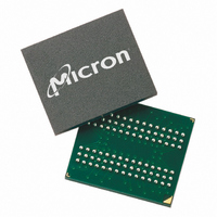
MT48H8M32LFB5-10 TR Micron Technology Inc, MT48H8M32LFB5-10 TR Datasheet - Page 37

MT48H8M32LFB5-10 TR
Manufacturer Part Number
MT48H8M32LFB5-10 TR
Description
IC SDRAM 256MBIT 100MHZ 90VFBGA
Manufacturer
Micron Technology Inc
Datasheet
1.MT48V8M32LFB5-8_IT_TR.pdf
(75 pages)
Specifications of MT48H8M32LFB5-10 TR
Format - Memory
RAM
Memory Type
Mobile SDRAM
Memory Size
256M (8Mx32)
Speed
100MHz
Interface
Parallel
Voltage - Supply
1.7 V ~ 1.95 V
Operating Temperature
0°C ~ 70°C
Package / Case
90-VFBGA
Lead Free Status / RoHS Status
Lead free / RoHS Compliant
CLOCK SUSPEND
BURST READ/SINGLE WRITE
Concurrent Auto Precharge
READ with Auto Precharge
PDF: 09005aef80d460f2/Source: 09005aef80cd8d41
256Mb SDRAM x32_2.fm - Rev. G 6/05
1. Interrupted by a READ (with or without auto precharge): A READ to bank m will inter-
2. Interrupted by a WRITE (with or without auto precharge): A WRITE to bank m will
The clock suspend mode occurs when a column access/burst is in progress and CKE is
registered LOW. In the clock suspend mode, the internal clock is deactivated, “freezing”
the synchronous logic.
For each positive clock edge on which CKE is sampled LOW, the next internal positive
clock edge is suspended. Any command or data present on the input balls at the time of
a suspended internal clock edge is ignored; any data present on the DQ balls remains
driven; and burst counters are not incremented, as long as the clock is suspended. (See
examples in Figure 25 and Figure 26.)
Clock suspend mode is exited by registering CKE HIGH; the internal clock and related
operation will resume on the subsequent positive clock edge.
The burst read/single write mode is entered by programming the write burst mode bit
(M9) in the mode register to a logic 1. In this mode, all WRITE commands result in the
access of a single column location (burst of one), regardless of the programmed burst
length. READ commands access columns according to the programmed burst length
and sequence, just as in the normal mode of operation (M9 = 0).
An access command (READ or WRITE) to a second bank while an access command with
auto precharge enabled on a first bank is executing is not allowed by SDRAMs, unless
the SDRAM supports concurrent auto precharge. Micron SDRAMs support concurrent
auto precharge. Four cases where concurrent auto precharge occurs are defined below.
rupt a READ on bank n, CAS latency later. The precharge to bank n will begin when
the READ to bank m is registered (Figure 27).
interrupt a READ on bank n when registered. DQM should be used two clocks prior to
the WRITE command to prevent bus contention. The precharge to bank n will begin
when the WRITE to bank m is registered (Figure 28).
37
Micron Technology, Inc., reserves the right to change products or specifications without notice.
256Mb: x32 Mobile SDRAM
©2003 Micron Technology, Inc. All rights reserved.
Operation


