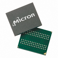
MT48H8M32LFB5-10 TR Micron Technology Inc, MT48H8M32LFB5-10 TR Datasheet - Page 27

MT48H8M32LFB5-10 TR
Manufacturer Part Number
MT48H8M32LFB5-10 TR
Description
IC SDRAM 256MBIT 100MHZ 90VFBGA
Manufacturer
Micron Technology Inc
Datasheet
1.MT48V8M32LFB5-8_IT_TR.pdf
(75 pages)
Specifications of MT48H8M32LFB5-10 TR
Format - Memory
RAM
Memory Type
Mobile SDRAM
Memory Size
256M (8Mx32)
Speed
100MHz
Interface
Parallel
Voltage - Supply
1.7 V ~ 1.95 V
Operating Temperature
0°C ~ 70°C
Package / Case
90-VFBGA
Lead Free Status / RoHS Status
Lead free / RoHS Compliant
PDF: 09005aef80d460f2/Source: 09005aef80cd8d41
256Mb SDRAM x32_2.fm - Rev. G 6/05
initiated on the clock edge immediately following the last (or last desired) data element
from the READ burst, provided that I/O contention can be avoided. In a given system
design, there may be a possibility that the device driving the input data will go Low-Z
before the SDRAM DQs go High-Z. In this case, at least a single-cycle delay should occur
between the last read data and the WRITE command.
The DQM input is used to avoid I/O contention, as shown in Figure 11 on page 26 and
Figure 12 on page 28. The DQM signal must be asserted (HIGH) at least two clocks prior
to the WRITE command (DQM latency is two clocks for output buffers) to suppress data-
out from the READ. Once the WRITE command is registered, the DQs will go High-Z (or
remain High-Z), regardless of the state of the DQM signal, provided the DQM was active
on the clock just prior to the WRITE command that truncated the READ command. If
not, the second WRITE will be an invalid WRITE. For example, if DQM was LOW during
T4 (in Figure 13) then the WRITEs at T5 and T7 would be valid, while the WRITE at T6
would be invalid.
The DQM signal must be de-asserted prior to the WRITE command (DQM latency is
zero clocks for input buffers) to ensure that the written data is not masked. Figure 12
shows the case where the clock frequency allows for bus contention to be avoided with-
out adding a NOP cycle, and Figure 13 shows the case where the additional NOP is
needed.
A fixed-length READ burst may be followed by, or truncated with, a PRECHARGE com-
mand to the same bank (provided that auto precharge was not activated), and a full-
page burst may be truncated with a PRECHARGE command to the same bank. The PRE-
CHARGE command should be issued x cycles before the clock edge at which the last
desired data element is valid, where x equals the CAS latency minus one. This is shown
in Figure 13 on page 28 for each possible CAS latency; data element n + 3 is either the last
of a burst of four or the last desired of a longer burst. Following the PRECHARGE com-
mand, a subsequent command to the same bank cannot be issued until
that part of the row precharge time is hidden during the access of the last data ele-
ment(s).
In the case of a fixed-length burst being executed to completion, a PRECHARGE com-
mand issued at the optimum time (as described above) provides the same operation
that would result from the same fixed-length burst with auto precharge. The disadvan-
tage of the PRECHARGE command is that it requires that the command and address
buses be available at the appropriate time to issue the command; the advantage of the
PRECHARGE command is that it can be used to truncate fixed-length or full-page
bursts.
27
Micron Technology, Inc., reserves the right to change products or specifications without notice.
256Mb: x32 Mobile SDRAM
©2003 Micron Technology, Inc. All rights reserved.
t
RP is met. Note
Operation


