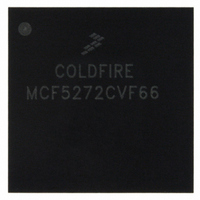
MCF5272CVF66 Freescale Semiconductor, MCF5272CVF66 Datasheet - Page 192

MCF5272CVF66
Manufacturer Part Number
MCF5272CVF66
Description
IC MPU 32BIT 66MHZ 196-MAPBGA
Manufacturer
Freescale Semiconductor
Series
MCF527xr
Specifications of MCF5272CVF66
Core Processor
Coldfire V2
Core Size
32-Bit
Speed
66MHz
Connectivity
EBI/EMI, Ethernet, I²C, SPI, UART/USART, USB
Peripherals
DMA, WDT
Number Of I /o
32
Program Memory Size
16KB (4K x 32)
Program Memory Type
ROM
Ram Size
1K x 32
Voltage - Supply (vcc/vdd)
3 V ~ 3.6 V
Oscillator Type
External
Operating Temperature
-40°C ~ 85°C
Package / Case
196-MAPBGA
Family Name
MCF5xxx
Device Core
ColdFire
Device Core Size
32b
Frequency (max)
66MHz
Instruction Set Architecture
RISC
Supply Voltage 1 (typ)
3.3V
Operating Temp Range
-40C to 85C
Operating Temperature Classification
Industrial
Mounting
Surface Mount
Pin Count
196
Package Type
MA-BGA
Lead Free Status / RoHS Status
Contains lead / RoHS non-compliant
Eeprom Size
-
Data Converters
-
Lead Free Status / Rohs Status
Not Compliant
Available stocks
Company
Part Number
Manufacturer
Quantity
Price
Company:
Part Number:
MCF5272CVF66
Manufacturer:
Freescale Semiconductor
Quantity:
10 000
Part Number:
MCF5272CVF66
Manufacturer:
FREESCALE
Quantity:
20 000
Company:
Part Number:
MCF5272CVF66 K75N
Manufacturer:
ST
Quantity:
18
Company:
Part Number:
MCF5272CVF66J
Manufacturer:
Freescale Semiconductor
Quantity:
10 000
- Current page: 192 of 544
- Download datasheet (7Mb)
SDRAM Controller
Table 9-1
9-2
A10_PRECHG
Internal 32-Bit Address Bus
DRESETEN
SDA[13:0]/
SDBA[1:0]
BS[3:0]
A[22:0]
Signal
CAS0
RAS0
describes SDRAM controller signals.
A10 precharge strobe. A precharge cycle occurs only after a page miss. During precharge, the SDRAM
writes the designated on-chip RAM page buffer back into the SDRAM array. Precharge latency is set
in SDTR[RP]. The reset value is 2 cycles, RP = 01.
For SDRAM devices, these outputs should be connected to individual DQM signals. During SDRAM
accesses, these signals indicate a byte transfer between SDRAM and the MCF5272 when asserted.
Note that most SDRAMs associate DQM3 with the MSB, in which case BS3 should be connected to
the SDRAM's DQM3 input, and so forth.
SDRAM column address strobe output
DRESETEN is asserted to indicate that the SDRAM controller is to be reset whenever RSTI asserts. If
DRESETEN is negated, RSTI does not affect the SDRAM controller, which continues to refresh
external memory. This is useful for debug situations where a reset of the device is required without
losing data located in SDRAM. DRESETEN is normally tied high or low depending on system
requirements. It should never be tied to RSTI or RSTO.
SDRAM row address strobe output
Fourteen address signals are multiplexed to form SDRAM_ADR[13:0], which are used for connecting
to SDRAM devices as large as 256 Mbits. SDRAM can be configured for 16- or 32-bit wide interface to
the MCF5272 data bus. For an SDRAM array with a 32-bit data bus, SDRAM address signals are
multiplexed starting with A2. For a 16-bit data bus, address signals are multiplexed starting with A1.
SDRAM controller bank address select outputs. Assigned to internal high-order address signals by
programming SDCR[BALOC]. This allows using SDRAM devices of different sizes without changing
the board layout. See
MCF5272 ColdFire
Table 9-1. SDRAM Controller Signal Descriptions
Figure 9-1. SDRAM Controller Signals
®
Address Multiplexer
Table
Dynamic Bus Sizer
SDRAM Controller
Integrated Microprocessor User’s Manual, Rev. 3
9-7.
10
32
1
1
1
1
4
2
1
1
1
8
2
Description
D[31:0]
SDRAMCS/CS7
RAS0
CAS0
SDWE
BS[3:0]
SDBA[1:0]
SDCLKE
SDCLK
A10_PRECHG
A[22:15]
A[11:2]/SDA[9:0]
A[14:13/SDA[12:11]
Freescale Semiconductor
Related parts for MCF5272CVF66
Image
Part Number
Description
Manufacturer
Datasheet
Request
R
Part Number:
Description:
Mcf5272 Coldfire Integrated Microprocessor User
Manufacturer:
Freescale Semiconductor, Inc
Datasheet:

Part Number:
Description:
MCF5272 Interrupt Service Routine for the Physical Layer Interface Controller
Manufacturer:
Freescale Semiconductor / Motorola
Datasheet:
Part Number:
Description:
Manufacturer:
Freescale Semiconductor, Inc
Datasheet:
Part Number:
Description:
Manufacturer:
Freescale Semiconductor, Inc
Datasheet:
Part Number:
Description:
Manufacturer:
Freescale Semiconductor, Inc
Datasheet:
Part Number:
Description:
Manufacturer:
Freescale Semiconductor, Inc
Datasheet:
Part Number:
Description:
Manufacturer:
Freescale Semiconductor, Inc
Datasheet:
Part Number:
Description:
Manufacturer:
Freescale Semiconductor, Inc
Datasheet:
Part Number:
Description:
Manufacturer:
Freescale Semiconductor, Inc
Datasheet:
Part Number:
Description:
Manufacturer:
Freescale Semiconductor, Inc
Datasheet:
Part Number:
Description:
Manufacturer:
Freescale Semiconductor, Inc
Datasheet:
Part Number:
Description:
Manufacturer:
Freescale Semiconductor, Inc
Datasheet:
Part Number:
Description:
Manufacturer:
Freescale Semiconductor, Inc
Datasheet:
Part Number:
Description:
Manufacturer:
Freescale Semiconductor, Inc
Datasheet:
Part Number:
Description:
Manufacturer:
Freescale Semiconductor, Inc
Datasheet:


