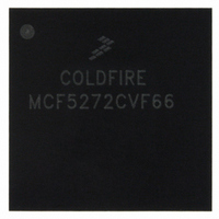
MCF5272CVF66 Freescale Semiconductor, MCF5272CVF66 Datasheet - Page 150

MCF5272CVF66
Manufacturer Part Number
MCF5272CVF66
Description
IC MPU 32BIT 66MHZ 196-MAPBGA
Manufacturer
Freescale Semiconductor
Series
MCF527xr
Specifications of MCF5272CVF66
Core Processor
Coldfire V2
Core Size
32-Bit
Speed
66MHz
Connectivity
EBI/EMI, Ethernet, I²C, SPI, UART/USART, USB
Peripherals
DMA, WDT
Number Of I /o
32
Program Memory Size
16KB (4K x 32)
Program Memory Type
ROM
Ram Size
1K x 32
Voltage - Supply (vcc/vdd)
3 V ~ 3.6 V
Oscillator Type
External
Operating Temperature
-40°C ~ 85°C
Package / Case
196-MAPBGA
Family Name
MCF5xxx
Device Core
ColdFire
Device Core Size
32b
Frequency (max)
66MHz
Instruction Set Architecture
RISC
Supply Voltage 1 (typ)
3.3V
Operating Temp Range
-40C to 85C
Operating Temperature Classification
Industrial
Mounting
Surface Mount
Pin Count
196
Package Type
MA-BGA
Lead Free Status / RoHS Status
Contains lead / RoHS non-compliant
Eeprom Size
-
Data Converters
-
Lead Free Status / Rohs Status
Not Compliant
Available stocks
Company
Part Number
Manufacturer
Quantity
Price
Company:
Part Number:
MCF5272CVF66
Manufacturer:
Freescale Semiconductor
Quantity:
10 000
Part Number:
MCF5272CVF66
Manufacturer:
FREESCALE
Quantity:
20 000
Company:
Part Number:
MCF5272CVF66 K75N
Manufacturer:
ST
Quantity:
18
Company:
Part Number:
MCF5272CVF66J
Manufacturer:
Freescale Semiconductor
Quantity:
10 000
- Current page: 150 of 544
- Download datasheet (7Mb)
Debug Support
Operand Data:
Result Data:
5.5.3.3.11
Read the selected debug module register and return the 32-bit result. The only valid register selection for
the
BKPT]; as well as the trigger status bits (CSR[BSTAT]) if either a level-2 breakpoint has been triggered
or a level-1 breakpoint has been triggered and no level-2 breakpoint has been enabled.
Command/Result Formats:
Table 5-20
Command Sequence:
Operand Data:
Result Data:
5-32
RDMREG
Command
0x01–0x1F
DRc[4:0]
0x00
Result
shows the definition of DRc encoding.
command is CSR (DRc = 0x00). Note that this read of the CSR clears CSR[FOF, TRG, HALT,
Read Debug Module Register (
15
MCF5272 ColdFire
This instruction requires two longword operands. The first selects the register to
which the operand data is to be written; the second contains the data.
Successful write operations return 0xFFFF. Bus errors on the write cycle are
indicated by the setting of bit 16 in the status message and by a data pattern of
0x0001.
None
The contents of the selected debug register are returned as a longword value. The
data is returned most-significant word first.
Debug Register Definition
0x2
Figure 5-37.
Configuration/Status
Table 5-20. Definition of DRc Encoding—Read
Reserved
Figure 5-38.
RDMREG
12
???
®
11
RDMREG BDM
Integrated Microprocessor User’s Manual, Rev. 3
RDMREG
0xD
MS RESULT
"ILLEGAL"
RDMREG
Command/Result Formats
Command Sequence
XXX
XXX
D[31:16]
8
D[15:0]
Mnemonic
7
)
CSR
—
100
"NOT READY"
LS RESULT
NEXT CMD
NEXT CMD
5
Initial State
4
0x0
—
Freescale Semiconductor
DRc
p. 5-10
Page
—
0
Related parts for MCF5272CVF66
Image
Part Number
Description
Manufacturer
Datasheet
Request
R
Part Number:
Description:
Mcf5272 Coldfire Integrated Microprocessor User
Manufacturer:
Freescale Semiconductor, Inc
Datasheet:

Part Number:
Description:
MCF5272 Interrupt Service Routine for the Physical Layer Interface Controller
Manufacturer:
Freescale Semiconductor / Motorola
Datasheet:
Part Number:
Description:
Manufacturer:
Freescale Semiconductor, Inc
Datasheet:
Part Number:
Description:
Manufacturer:
Freescale Semiconductor, Inc
Datasheet:
Part Number:
Description:
Manufacturer:
Freescale Semiconductor, Inc
Datasheet:
Part Number:
Description:
Manufacturer:
Freescale Semiconductor, Inc
Datasheet:
Part Number:
Description:
Manufacturer:
Freescale Semiconductor, Inc
Datasheet:
Part Number:
Description:
Manufacturer:
Freescale Semiconductor, Inc
Datasheet:
Part Number:
Description:
Manufacturer:
Freescale Semiconductor, Inc
Datasheet:
Part Number:
Description:
Manufacturer:
Freescale Semiconductor, Inc
Datasheet:
Part Number:
Description:
Manufacturer:
Freescale Semiconductor, Inc
Datasheet:
Part Number:
Description:
Manufacturer:
Freescale Semiconductor, Inc
Datasheet:
Part Number:
Description:
Manufacturer:
Freescale Semiconductor, Inc
Datasheet:
Part Number:
Description:
Manufacturer:
Freescale Semiconductor, Inc
Datasheet:
Part Number:
Description:
Manufacturer:
Freescale Semiconductor, Inc
Datasheet:


