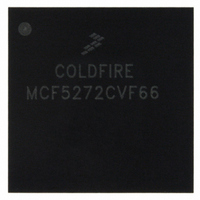
MCF5272CVF66 Freescale Semiconductor, MCF5272CVF66 Datasheet - Page 189

MCF5272CVF66
Manufacturer Part Number
MCF5272CVF66
Description
IC MPU 32BIT 66MHZ 196-MAPBGA
Manufacturer
Freescale Semiconductor
Series
MCF527xr
Specifications of MCF5272CVF66
Core Processor
Coldfire V2
Core Size
32-Bit
Speed
66MHz
Connectivity
EBI/EMI, Ethernet, I²C, SPI, UART/USART, USB
Peripherals
DMA, WDT
Number Of I /o
32
Program Memory Size
16KB (4K x 32)
Program Memory Type
ROM
Ram Size
1K x 32
Voltage - Supply (vcc/vdd)
3 V ~ 3.6 V
Oscillator Type
External
Operating Temperature
-40°C ~ 85°C
Package / Case
196-MAPBGA
Family Name
MCF5xxx
Device Core
ColdFire
Device Core Size
32b
Frequency (max)
66MHz
Instruction Set Architecture
RISC
Supply Voltage 1 (typ)
3.3V
Operating Temp Range
-40C to 85C
Operating Temperature Classification
Industrial
Mounting
Surface Mount
Pin Count
196
Package Type
MA-BGA
Lead Free Status / RoHS Status
Contains lead / RoHS non-compliant
Eeprom Size
-
Data Converters
-
Lead Free Status / Rohs Status
Not Compliant
Available stocks
Company
Part Number
Manufacturer
Quantity
Price
Company:
Part Number:
MCF5272CVF66
Manufacturer:
Freescale Semiconductor
Quantity:
10 000
Part Number:
MCF5272CVF66
Manufacturer:
FREESCALE
Quantity:
20 000
Company:
Part Number:
MCF5272CVF66 K75N
Manufacturer:
ST
Quantity:
18
Company:
Part Number:
MCF5272CVF66J
Manufacturer:
Freescale Semiconductor
Quantity:
10 000
- Current page: 189 of 544
- Download datasheet (7Mb)
8.2.2
CSOR0–CSOR7,
capability, wait states, and read/write access.
Table 8-5
Freescale Semiconductor
31–12
Name
11
10
Reset
Field
Addr
R/W
31
describes CSORn fields.
WRAH
Name
ASET
BAM
Chip Select Option Registers (CSOR0–CSOR7)
Figure
BAM
Address mask. Masks equivalent CSOR[BA] bits. The BAM setting chooses which BA bits to compare
with the corresponding address bit to determine a match.
0 Mask address bit
1 Compare address bit
Address setup enable. Controls assertion of chip select with respect to assertion of a valid address that
hits in the chip select address space.
0 Assert chip select on the rising edge of CLK that address is asserted.
1 Delay assertion of chip select for one CLK cycle after address is asserted. During write transfers,
R/W asserts 1 clock cycle after assertion of the chip select.
Controls the address, data, and attribute hold time after the termination, internal or external with TA, of
a write cycle that hits in the chip select address space.
0 Do not hold address, data, and attribute signals an extra cycle after chip select and R/W negate on
1 Hold address, data, and attribute signals an extra cycle after CSx and R/W negate on writes.
MCF5272 ColdFire
both chip select and R/W are delayed by 1 clock cycle.
writes.
Table 8-4. Chip Select Memory Address Decoding Priority
8-2, are used to configure the address mask, additional setup/hold, extended burst
0x044 (CSOR0); 0x04C (CSOR1); 0x054 (CSOR2); 0x05C (CSOR3);
0x064 (CSOR4); 0x06C (CSOR5); 0x074 (CSOR6); 0x07C (CSOR7)
Figure 8-2. Chip Select Option Registers (CSORn)
12
Table 8-5. CSORn Field Descriptions
ASET WRAH RDAH EXTBURST
11
®
Priority
Highest
Lowest
Integrated Microprocessor User’s Manual, Rev. 3
10
0xFFFF_F078
9
R/W
Chip select 1
Chip select 2
Chip select 3
Chip select 4
Chip select 5
Chip select 6
Description
Chip select 0
Chip select 7
Chip Select
8
—
7
6
WS
2
RW
Chip Select Module
1
MRW
0
8-5
Related parts for MCF5272CVF66
Image
Part Number
Description
Manufacturer
Datasheet
Request
R
Part Number:
Description:
Mcf5272 Coldfire Integrated Microprocessor User
Manufacturer:
Freescale Semiconductor, Inc
Datasheet:

Part Number:
Description:
MCF5272 Interrupt Service Routine for the Physical Layer Interface Controller
Manufacturer:
Freescale Semiconductor / Motorola
Datasheet:
Part Number:
Description:
Manufacturer:
Freescale Semiconductor, Inc
Datasheet:
Part Number:
Description:
Manufacturer:
Freescale Semiconductor, Inc
Datasheet:
Part Number:
Description:
Manufacturer:
Freescale Semiconductor, Inc
Datasheet:
Part Number:
Description:
Manufacturer:
Freescale Semiconductor, Inc
Datasheet:
Part Number:
Description:
Manufacturer:
Freescale Semiconductor, Inc
Datasheet:
Part Number:
Description:
Manufacturer:
Freescale Semiconductor, Inc
Datasheet:
Part Number:
Description:
Manufacturer:
Freescale Semiconductor, Inc
Datasheet:
Part Number:
Description:
Manufacturer:
Freescale Semiconductor, Inc
Datasheet:
Part Number:
Description:
Manufacturer:
Freescale Semiconductor, Inc
Datasheet:
Part Number:
Description:
Manufacturer:
Freescale Semiconductor, Inc
Datasheet:
Part Number:
Description:
Manufacturer:
Freescale Semiconductor, Inc
Datasheet:
Part Number:
Description:
Manufacturer:
Freescale Semiconductor, Inc
Datasheet:
Part Number:
Description:
Manufacturer:
Freescale Semiconductor, Inc
Datasheet:


