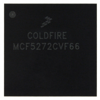
MCF5272CVF66 Freescale Semiconductor, MCF5272CVF66 Datasheet - Page 130

MCF5272CVF66
Manufacturer Part Number
MCF5272CVF66
Description
IC MPU 32BIT 66MHZ 196-MAPBGA
Manufacturer
Freescale Semiconductor
Series
MCF527xr
Specifications of MCF5272CVF66
Core Processor
Coldfire V2
Core Size
32-Bit
Speed
66MHz
Connectivity
EBI/EMI, Ethernet, I²C, SPI, UART/USART, USB
Peripherals
DMA, WDT
Number Of I /o
32
Program Memory Size
16KB (4K x 32)
Program Memory Type
ROM
Ram Size
1K x 32
Voltage - Supply (vcc/vdd)
3 V ~ 3.6 V
Oscillator Type
External
Operating Temperature
-40°C ~ 85°C
Package / Case
196-MAPBGA
Family Name
MCF5xxx
Device Core
ColdFire
Device Core Size
32b
Frequency (max)
66MHz
Instruction Set Architecture
RISC
Supply Voltage 1 (typ)
3.3V
Operating Temp Range
-40C to 85C
Operating Temperature Classification
Industrial
Mounting
Surface Mount
Pin Count
196
Package Type
MA-BGA
Lead Free Status / RoHS Status
Contains lead / RoHS non-compliant
Eeprom Size
-
Data Converters
-
Lead Free Status / Rohs Status
Not Compliant
Available stocks
Company
Part Number
Manufacturer
Quantity
Price
Company:
Part Number:
MCF5272CVF66
Manufacturer:
Freescale Semiconductor
Quantity:
10 000
Part Number:
MCF5272CVF66
Manufacturer:
FREESCALE
Quantity:
20 000
Company:
Part Number:
MCF5272CVF66 K75N
Manufacturer:
ST
Quantity:
18
Company:
Part Number:
MCF5272CVF66J
Manufacturer:
Freescale Semiconductor
Quantity:
10 000
- Current page: 130 of 544
- Download datasheet (7Mb)
Debug Support
5.4.5
The data breakpoint register (DBR),
mode. DBR bits are masked by setting corresponding DBMR bits, as defined in TDR.
Table 5-9
Table 5-10
The DBR supports both aligned and misaligned references.
processor address, access size, and location within the 32-bit data bus.
5-12
31–0
31–0
Bits
Bits
DRc[4–0]
Reset
Field
R/W DBR is accessible in supervisor mode as debug control register 0x0E, using the WDEBUG instruction and
Name
Name
Data
Mask
describes DBR fields.
describes DBMR fields.
Data Breakpoint/Mask Registers (DBR, DBMR)
through the BDM port using the
DBMR is accessible in supervisor mode as debug control register 0x0F,using the WDEBUG instruction and
via the BDM port using the
31
Data breakpoint value. Contains the value to be compared with the data value from the processor’s local bus
as a breakpoint trigger.
Data breakpoint mask. The 32-bit mask for the data breakpoint trigger. Clearing a DBR bit allows the
corresponding DBR bit to be compared to the appropriate bit of the processor’s local data bus. Setting a
DBMR bit causes that bit to be ignored.
MCF5272 ColdFire
Figure 5-8. Data Breakpoint/Mask Registers (DBR and DBMR)
Table 5-11. Access Size and Operand Data Location
A[1:0]
00
01
10
11
0x
1x
xx
Table 5-10. DBMR Field Descriptions
WDMREG
Table 5-9. DBR Field Descriptions
Figure
®
RDMREG
Integrated Microprocessor User’s Manual, Rev. 3
command.
5-8, specify data patterns used as part of the trigger into debug
Access Size
Data (DBR); Mask (DBMR)
0x0E (DBR), 0x0F (DBMR)
and
Longword
Word
Word
Byte
Byte
Byte
Byte
WDMREG
Uninitialized
Description
Description
commands.
Table 5-11
Operand Location
D[31:24]
D[23:16]
D[31:16]
D[15:8]
D[15:0]
D[31:0]
D[7:0]
shows relationships between
Freescale Semiconductor
0
Related parts for MCF5272CVF66
Image
Part Number
Description
Manufacturer
Datasheet
Request
R
Part Number:
Description:
Mcf5272 Coldfire Integrated Microprocessor User
Manufacturer:
Freescale Semiconductor, Inc
Datasheet:

Part Number:
Description:
MCF5272 Interrupt Service Routine for the Physical Layer Interface Controller
Manufacturer:
Freescale Semiconductor / Motorola
Datasheet:
Part Number:
Description:
Manufacturer:
Freescale Semiconductor, Inc
Datasheet:
Part Number:
Description:
Manufacturer:
Freescale Semiconductor, Inc
Datasheet:
Part Number:
Description:
Manufacturer:
Freescale Semiconductor, Inc
Datasheet:
Part Number:
Description:
Manufacturer:
Freescale Semiconductor, Inc
Datasheet:
Part Number:
Description:
Manufacturer:
Freescale Semiconductor, Inc
Datasheet:
Part Number:
Description:
Manufacturer:
Freescale Semiconductor, Inc
Datasheet:
Part Number:
Description:
Manufacturer:
Freescale Semiconductor, Inc
Datasheet:
Part Number:
Description:
Manufacturer:
Freescale Semiconductor, Inc
Datasheet:
Part Number:
Description:
Manufacturer:
Freescale Semiconductor, Inc
Datasheet:
Part Number:
Description:
Manufacturer:
Freescale Semiconductor, Inc
Datasheet:
Part Number:
Description:
Manufacturer:
Freescale Semiconductor, Inc
Datasheet:
Part Number:
Description:
Manufacturer:
Freescale Semiconductor, Inc
Datasheet:
Part Number:
Description:
Manufacturer:
Freescale Semiconductor, Inc
Datasheet:


