DEMO9S08JM16 Freescale Semiconductor, DEMO9S08JM16 Datasheet - Page 75
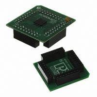
DEMO9S08JM16
Manufacturer Part Number
DEMO9S08JM16
Description
BOARD DEMO FOR JM16 FAMI
Manufacturer
Freescale Semiconductor
Type
MCUr
Datasheets
1.DEMO9S08JM16.pdf
(47 pages)
2.DEMO9S08JM16.pdf
(5 pages)
3.DEMO9S08JM16.pdf
(4 pages)
4.DEMO9S08JM16.pdf
(386 pages)
Specifications of DEMO9S08JM16
Contents
Board with Daughter card, Cable, Documentation, Mini-AB USB Kit
Processor To Be Evaluated
MC9S08JM16
Data Bus Width
8 bit
Interface Type
USB
Silicon Manufacturer
Freescale
Core Architecture
HCS08
Core Sub-architecture
HCS08
Silicon Core Number
MC9S08
Silicon Family Name
Flexis - S08JM
Rohs Compliant
Yes
For Use With/related Products
MC9S08JM16
Lead Free Status / RoHS Status
Lead free / RoHS Compliant


5.7.8
This register is used to report the status of the low-voltage warning function, and to configure the stop
mode behavior of the MCU. This register must be written during the user’s reset initialization program to
set the desired controls even if the desired settings are the same as the reset settings.
Freescale Semiconductor
Any other Reset:
1
Power-on Reset:
This bit can be written only one time after reset. Additional writes are ignored.
PPDACK
PPDC
LVWV
PPDF
LVD Reset:
LVDV
Field
5
4
3
2
0
System Power Management Status and Control 2 Register
(SPMSC2)
Figure 5-10. System Power Management Status and Control 2 Register (SPMSC2)
W
R
Low-Voltage Detect Voltage Select — This write-once bit selects the low-voltage detect (LVD) trip point
setting. It also selects the warning voltage range. See
Low-Voltage Warning Voltage Select — This bit selects the low-voltage warning (LVW) trip point
voltage.See
Partial Power Down Flag — This read-only status bit indicates that the MCU has recovered from stop2
mode.
0 MCU has not recovered from stop2 mode.
1 MCU recovered from stop2 mode.
Partial Power Down Acknowledge — Writing a 1 to PPDACK clears the PPDF bit.
Partial Power Down Control — This write-once bit controls whether stop2 or stop3 mode is selected.
0 Stop3 mode enabled.
1 Stop2, partial power down, mode enabled.
1
See Electrical Characteristics appendix for minimum and maximum values.
0
0
0
0
7
LVDV:LVWV
Table
0:0
0:1
1:0
1:1
= Unimplemented or Reserved
Table 5-12. LVD and LVW Trip Point Typical Values
Table 5-11. SPMSC2 Register Field Descriptions
5-12.
0
0
0
0
6
MC9S08JM16 Series Data Sheet, Rev. 2
LVDV
0
u
u
5
LVW Trip Point
V
V
V
V
LVW0
LVW1
LVW2
LVW3
= 2.74 V
= 2.92 V
= 4.3 V
= 4.6 V
LVWV
4
0
u
u
Description
Table
Chapter 5 Resets, Interrupts, and System Configuration
PPDF
0
0
0
3
5-12.
LVD Trip Point
V
V
LVD0
LVD1
u = Unaffected by reset
PPDACK
= 2.56 V
= 4.0 V
0
0
0
0
2
1
0
0
0
0
1
PPDC
0
0
0
0
1
75
Related parts for DEMO9S08JM16
Image
Part Number
Description
Manufacturer
Datasheet
Request
R

Part Number:
Description:
Manufacturer:
Freescale Semiconductor, Inc
Datasheet:
Part Number:
Description:
Manufacturer:
Freescale Semiconductor, Inc
Datasheet:
Part Number:
Description:
Manufacturer:
Freescale Semiconductor, Inc
Datasheet:
Part Number:
Description:
Manufacturer:
Freescale Semiconductor, Inc
Datasheet:
Part Number:
Description:
Manufacturer:
Freescale Semiconductor, Inc
Datasheet:
Part Number:
Description:
Manufacturer:
Freescale Semiconductor, Inc
Datasheet:
Part Number:
Description:
Manufacturer:
Freescale Semiconductor, Inc
Datasheet:
Part Number:
Description:
Manufacturer:
Freescale Semiconductor, Inc
Datasheet:
Part Number:
Description:
Manufacturer:
Freescale Semiconductor, Inc
Datasheet:
Part Number:
Description:
Manufacturer:
Freescale Semiconductor, Inc
Datasheet:
Part Number:
Description:
Manufacturer:
Freescale Semiconductor, Inc
Datasheet:
Part Number:
Description:
Manufacturer:
Freescale Semiconductor, Inc
Datasheet:
Part Number:
Description:
Manufacturer:
Freescale Semiconductor, Inc
Datasheet:
Part Number:
Description:
Manufacturer:
Freescale Semiconductor, Inc
Datasheet:
Part Number:
Description:
Manufacturer:
Freescale Semiconductor, Inc
Datasheet: