DEMO9S08JM16 Freescale Semiconductor, DEMO9S08JM16 Datasheet - Page 257
DEMO9S08JM16
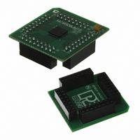
Manufacturer Part Number
DEMO9S08JM16
Description
BOARD DEMO FOR JM16 FAMI
Manufacturer
Freescale Semiconductor
Type
MCUr
Datasheets
1.DEMO9S08JM16.pdf
(47 pages)
2.DEMO9S08JM16.pdf
(5 pages)
3.DEMO9S08JM16.pdf
(4 pages)
4.DEMO9S08JM16.pdf
(386 pages)
Specifications of DEMO9S08JM16
Contents
Board with Daughter card, Cable, Documentation, Mini-AB USB Kit
Processor To Be Evaluated
MC9S08JM16
Data Bus Width
8 bit
Interface Type
USB
Silicon Manufacturer
Freescale
Core Architecture
HCS08
Core Sub-architecture
HCS08
Silicon Core Number
MC9S08
Silicon Family Name
Flexis - S08JM
Rohs Compliant
Yes
For Use With/related Products
MC9S08JM16
Lead Free Status / RoHS Status
Lead free / RoHS Compliant


SPSCK cycle after the end of the eighth bit time of the transfer. The SS IN waveform applies to the slave
select input of a slave.
When CPHA = 0, the slave begins to drive its MISO output with the first data bit value (MSB or LSB
depending on LSBFE) when SS goes to active low. The first SPSCK edge causes both the master and the
slave to sample the data bit values on their MISO and MOSI inputs, respectively. At the second SPSCK
edge, the SPI shifter shifts one bit position which shifts in the bit value that was just sampled and shifts the
second data bit value out the other end of the shifter to the MOSI and MISO outputs of the master and
slave, respectively. When CPHA = 0, the slave’s SS input must go to its inactive high level between
transfers.
15.4.6
As shown in
prescale bits (SPPR2:SPPR1:SPPR0) choose a prescale divisor of 1, 2, 3, 4, 5, 6, 7, or 8. The three rate
select bits (SPR2:SPR1:SPR0) divide the output of the prescaler stage by 2, 4, 8, 16, 32, 64, 128, or 256
to get the internal SPI master mode bit-rate clock.
The baud rate generator is activated only when the SPI is in the master mode and a serial transfer is taking
place. In the other cases, the divider is disabled to decrease I
Freescale Semiconductor
(MISO OR MOSI)
(MASTER OUT)
(REFERENCE)
(SLAVE OUT)
SAMPLE IN
MSB FIRST
BIT TIME #
(CPOL = 0)
(CPOL = 1)
LSB FIRST
(MASTER)
(SLAVE)
SS OUT
SPSCK
SPSCK
SS IN
MOSI
MISO
SPI Baud Rate Generation
Figure
15-15, the clock source for the SPI baud rate generator is the bus clock. The three
BIT 7
BIT 0
1
Figure 15-14. SPI Clock Formats (CPHA = 0)
MC9S08JM16 Series Data Sheet, Rev. 2
BIT 6
BIT 1
2
...
...
...
BIT 2
BIT 5
DD
6
current.
BIT 1
BIT 6
7
Serial Peripheral Interface (S08SPI16V1)
BIT 0
BIT 7
8
257
Related parts for DEMO9S08JM16
Image
Part Number
Description
Manufacturer
Datasheet
Request
R

Part Number:
Description:
Manufacturer:
Freescale Semiconductor, Inc
Datasheet:
Part Number:
Description:
Manufacturer:
Freescale Semiconductor, Inc
Datasheet:
Part Number:
Description:
Manufacturer:
Freescale Semiconductor, Inc
Datasheet:
Part Number:
Description:
Manufacturer:
Freescale Semiconductor, Inc
Datasheet:
Part Number:
Description:
Manufacturer:
Freescale Semiconductor, Inc
Datasheet:
Part Number:
Description:
Manufacturer:
Freescale Semiconductor, Inc
Datasheet:
Part Number:
Description:
Manufacturer:
Freescale Semiconductor, Inc
Datasheet:
Part Number:
Description:
Manufacturer:
Freescale Semiconductor, Inc
Datasheet:
Part Number:
Description:
Manufacturer:
Freescale Semiconductor, Inc
Datasheet:
Part Number:
Description:
Manufacturer:
Freescale Semiconductor, Inc
Datasheet:
Part Number:
Description:
Manufacturer:
Freescale Semiconductor, Inc
Datasheet:
Part Number:
Description:
Manufacturer:
Freescale Semiconductor, Inc
Datasheet:
Part Number:
Description:
Manufacturer:
Freescale Semiconductor, Inc
Datasheet:
Part Number:
Description:
Manufacturer:
Freescale Semiconductor, Inc
Datasheet:
Part Number:
Description:
Manufacturer:
Freescale Semiconductor, Inc
Datasheet: