DEMO9S08JM16 Freescale Semiconductor, DEMO9S08JM16 Datasheet - Page 254
DEMO9S08JM16
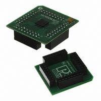
Manufacturer Part Number
DEMO9S08JM16
Description
BOARD DEMO FOR JM16 FAMI
Manufacturer
Freescale Semiconductor
Type
MCUr
Datasheets
1.DEMO9S08JM16.pdf
(47 pages)
2.DEMO9S08JM16.pdf
(5 pages)
3.DEMO9S08JM16.pdf
(4 pages)
4.DEMO9S08JM16.pdf
(386 pages)
Specifications of DEMO9S08JM16
Contents
Board with Daughter card, Cable, Documentation, Mini-AB USB Kit
Processor To Be Evaluated
MC9S08JM16
Data Bus Width
8 bit
Interface Type
USB
Silicon Manufacturer
Freescale
Core Architecture
HCS08
Core Sub-architecture
HCS08
Silicon Core Number
MC9S08
Silicon Family Name
Flexis - S08JM
Rohs Compliant
Yes
For Use With/related Products
MC9S08JM16
Lead Free Status / RoHS Status
Lead free / RoHS Compliant


Serial Peripheral Interface (S08SPI16V1)
As long as no more than one slave device drives the system slave’s serial data output line, it is possible for
several slaves to receive the same transmission from a master, although the master would not receive return
information from all of the receiving slaves.
If the CPHA bit in SPI Control Register 1 is clear, odd numbered edges on the SPSCK input cause the data
at the serial data input pin to be latched. Even numbered edges cause the value previously latched from the
serial data input pin to shift into the LSB or MSB of the SPI shift register, depending on the LSBFE bit.
If the CPHA bit is set, even numbered edges on the SPSCK input cause the data at the serial data input pin
to be latched. Odd numbered edges cause the value previously latched from the serial data input pin to shift
into the LSB or MSB of the SPI shift register, depending on the LSBFE bit.
When CPHA is set, the first edge is used to get the first data bit onto the serial data output pin. When CPHA
is clear and the SS input is low (slave selected), the first bit of the SPI data is driven out of the serial data
output pin. After the eighth (SPIMODE = 0) or sixteenth (SPIMODE = 1) shift, the transfer is considered
complete and the received data is transferred into the SPI data registers. To indicate transfer is complete,
the SPRF flag in the SPI Status Register is set.
15.4.4
The SPI can support data lengths of 8 or 16 bits. The length can be configured with the SPIMODE bit in
the SPIxC2 register.
In 8-bit mode (SPIMODE = 0), the SPI Data Register is comprised of one byte: SPIxDL. The SPI Match
Register is also comprised of only one byte: SPIxML. Reads of SPIxDH and SPIxMH will return zero.
Writes to SPIxDH and SPIxMH will be ignored.
In 16-bit mode (SPIMODE = 1), the SPI Data Register is comprised of two bytes: SPIxDH and SPIxDL.
Reading either byte (SPIxDH or SPIxDL) latches the contents of both bytes into a buffer where they
remain latched until the other byte is read. Writing to either byte (SPIxDH or SPIxDL) latches the value
into a buffer. When both bytes have been written, they are transferred as a coherent 16-bit value into the
transmit data buffer.
In 16-bit mode, the SPI Match Register is also comprised of two bytes: SPIxMH and SPIxML. Reading
either byte (SPIxMH or SPIxML) latches the contents of both bytes into a buffer where they remain latched
until the other byte is read. Writing to either byte (SPIxMH or SPIxML) latches the value into a buffer.
When both bytes have been written, they are transferred as a coherent 16-bit value into the transmit data
buffer.
254
Data Transmission Length
When peripherals with duplex capability are used, take care not to
simultaneously enable two receivers whose serial outputs drive the same
system slave’s serial data output line.
A change of the bits CPOL, CPHA, SSOE, LSBFE, MODFEN, SPC0 and
BIDIROE with SPC0 set and SPIMODE in slave mode will corrupt a
transmission in progress and has to be avoided.
MC9S08JM16 Series Data Sheet, Rev. 2
NOTE
NOTE
Freescale Semiconductor
Related parts for DEMO9S08JM16
Image
Part Number
Description
Manufacturer
Datasheet
Request
R

Part Number:
Description:
Manufacturer:
Freescale Semiconductor, Inc
Datasheet:
Part Number:
Description:
Manufacturer:
Freescale Semiconductor, Inc
Datasheet:
Part Number:
Description:
Manufacturer:
Freescale Semiconductor, Inc
Datasheet:
Part Number:
Description:
Manufacturer:
Freescale Semiconductor, Inc
Datasheet:
Part Number:
Description:
Manufacturer:
Freescale Semiconductor, Inc
Datasheet:
Part Number:
Description:
Manufacturer:
Freescale Semiconductor, Inc
Datasheet:
Part Number:
Description:
Manufacturer:
Freescale Semiconductor, Inc
Datasheet:
Part Number:
Description:
Manufacturer:
Freescale Semiconductor, Inc
Datasheet:
Part Number:
Description:
Manufacturer:
Freescale Semiconductor, Inc
Datasheet:
Part Number:
Description:
Manufacturer:
Freescale Semiconductor, Inc
Datasheet:
Part Number:
Description:
Manufacturer:
Freescale Semiconductor, Inc
Datasheet:
Part Number:
Description:
Manufacturer:
Freescale Semiconductor, Inc
Datasheet:
Part Number:
Description:
Manufacturer:
Freescale Semiconductor, Inc
Datasheet:
Part Number:
Description:
Manufacturer:
Freescale Semiconductor, Inc
Datasheet:
Part Number:
Description:
Manufacturer:
Freescale Semiconductor, Inc
Datasheet: