DEMO9S08JM16 Freescale Semiconductor, DEMO9S08JM16 Datasheet - Page 346
DEMO9S08JM16
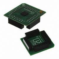
Manufacturer Part Number
DEMO9S08JM16
Description
BOARD DEMO FOR JM16 FAMI
Manufacturer
Freescale Semiconductor
Type
MCUr
Datasheets
1.DEMO9S08JM16.pdf
(47 pages)
2.DEMO9S08JM16.pdf
(5 pages)
3.DEMO9S08JM16.pdf
(4 pages)
4.DEMO9S08JM16.pdf
(386 pages)
Specifications of DEMO9S08JM16
Contents
Board with Daughter card, Cable, Documentation, Mini-AB USB Kit
Processor To Be Evaluated
MC9S08JM16
Data Bus Width
8 bit
Interface Type
USB
Silicon Manufacturer
Freescale
Core Architecture
HCS08
Core Sub-architecture
HCS08
Silicon Core Number
MC9S08
Silicon Family Name
Flexis - S08JM
Rohs Compliant
Yes
For Use With/related Products
MC9S08JM16
Lead Free Status / RoHS Status
Lead free / RoHS Compliant


Development Support
18.4.3.7
This register can be read or written at any time.
346
Reset
RWBEN
DBGEN
RWAEN
BRKEN
Field
ARM
RWA
RWB
TAG
W
7
6
5
4
3
2
1
0
R
DBGEN
Debug Module Enable — Used to enable the debug module. DBGEN cannot be set to 1 if the MCU is secure.
0 DBG disabled
1 DBG enabled
Arm Control — Controls whether the debugger is comparing and storing information in the FIFO. A write is used
to set this bit (and ARMF) and completion of a debug run automatically clears it. Any debug run can be manually
stopped by writing 0 to ARM or to DBGEN.
0 Debugger not armed
1 Debugger armed
Tag/Force Select — Controls whether break requests to the CPU will be tag or force type requests. If
BRKEN = 0, this bit has no meaning or effect.
0 CPU breaks requested as force type requests
1 CPU breaks requested as tag type requests
Break Enable — Controls whether a trigger event will generate a break request to the CPU. Trigger events can
cause information to be stored in the FIFO without generating a break request to the CPU. For an end trace, CPU
break requests are issued to the CPU when the comparator(s) and R/W meet the trigger requirements. For a
begin trace, CPU break requests are issued when the FIFO becomes full. TRGSEL does not affect the timing of
CPU break requests.
0 CPU break requests not enabled
1 Triggers cause a break request to the CPU
R/W Comparison Value for Comparator A — When RWAEN = 1, this bit determines whether a read or a write
access qualifies comparator A. When RWAEN = 0, RWA and the R/W signal do not affect comparator A.
0 Comparator A can only match on a write cycle
1 Comparator A can only match on a read cycle
Enable R/W for Comparator A — Controls whether the level of R/W is considered for a comparator A match.
0 R/W is not used in comparison A
1 R/W is used in comparison A
R/W Comparison Value for Comparator B — When RWBEN = 1, this bit determines whether a read or a write
access qualifies comparator B. When RWBEN = 0, RWB and the R/W signal do not affect comparator B.
0 Comparator B can match only on a write cycle
1 Comparator B can match only on a read cycle
Enable R/W for Comparator B — Controls whether the level of R/W is considered for a comparator B match.
0 R/W is not used in comparison B
1 R/W is used in comparison B
0
7
Debug Control Register (DBGC)
ARM
0
6
Table 18-4. DBGC Register Field Descriptions
Figure 18-7. Debug Control Register (DBGC)
MC9S08JM16 Series Data Sheet, Rev. 2
TAG
0
5
BRKEN
0
4
Description
RWA
0
3
RWAEN
0
2
Freescale Semiconductor
RWB
1
0
RWBEN
0
0
Related parts for DEMO9S08JM16
Image
Part Number
Description
Manufacturer
Datasheet
Request
R

Part Number:
Description:
Manufacturer:
Freescale Semiconductor, Inc
Datasheet:
Part Number:
Description:
Manufacturer:
Freescale Semiconductor, Inc
Datasheet:
Part Number:
Description:
Manufacturer:
Freescale Semiconductor, Inc
Datasheet:
Part Number:
Description:
Manufacturer:
Freescale Semiconductor, Inc
Datasheet:
Part Number:
Description:
Manufacturer:
Freescale Semiconductor, Inc
Datasheet:
Part Number:
Description:
Manufacturer:
Freescale Semiconductor, Inc
Datasheet:
Part Number:
Description:
Manufacturer:
Freescale Semiconductor, Inc
Datasheet:
Part Number:
Description:
Manufacturer:
Freescale Semiconductor, Inc
Datasheet:
Part Number:
Description:
Manufacturer:
Freescale Semiconductor, Inc
Datasheet:
Part Number:
Description:
Manufacturer:
Freescale Semiconductor, Inc
Datasheet:
Part Number:
Description:
Manufacturer:
Freescale Semiconductor, Inc
Datasheet:
Part Number:
Description:
Manufacturer:
Freescale Semiconductor, Inc
Datasheet:
Part Number:
Description:
Manufacturer:
Freescale Semiconductor, Inc
Datasheet:
Part Number:
Description:
Manufacturer:
Freescale Semiconductor, Inc
Datasheet:
Part Number:
Description:
Manufacturer:
Freescale Semiconductor, Inc
Datasheet: