DEMO9S08JM16 Freescale Semiconductor, DEMO9S08JM16 Datasheet - Page 149
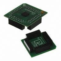
DEMO9S08JM16
Manufacturer Part Number
DEMO9S08JM16
Description
BOARD DEMO FOR JM16 FAMI
Manufacturer
Freescale Semiconductor
Type
MCUr
Datasheets
1.DEMO9S08JM16.pdf
(47 pages)
2.DEMO9S08JM16.pdf
(5 pages)
3.DEMO9S08JM16.pdf
(4 pages)
4.DEMO9S08JM16.pdf
(386 pages)
Specifications of DEMO9S08JM16
Contents
Board with Daughter card, Cable, Documentation, Mini-AB USB Kit
Processor To Be Evaluated
MC9S08JM16
Data Bus Width
8 bit
Interface Type
USB
Silicon Manufacturer
Freescale
Core Architecture
HCS08
Core Sub-architecture
HCS08
Silicon Core Number
MC9S08
Silicon Family Name
Flexis - S08JM
Rohs Compliant
Yes
For Use With/related Products
MC9S08JM16
Lead Free Status / RoHS Status
Lead free / RoHS Compliant


If continuous conversions are enabled, a new conversion is automatically initiated after the completion of
the current conversion. In software triggered operation, continuous conversions begin after ADCSC1 is
written and continue until aborted. In hardware triggered operation, continuous conversions begin after a
hardware trigger event and continue until aborted.
10.4.4.2
A conversion is completed when the result of the conversion is transferred into the data result registers,
ADCRH and ADCRL. This is indicated by the setting of COCO. An interrupt is generated if AIEN is high
at the time that COCO is set.
A blocking mechanism prevents a new result from overwriting previous data in ADCRH and ADCRL if
the previous data is in the process of being read while in 12-bit or 10-bit MODE (the ADCRH register has
been read but the ADCRL register has not). When blocking is active, the data transfer is blocked, COCO
is not set, and the new result is lost. In the case of single conversions with the compare function enabled
and the compare condition false, blocking has no effect and ADC operation is terminated. In all other cases
of operation, when a data transfer is blocked, another conversion is initiated regardless of the state of
ADCO (single or continuous conversions enabled).
If single conversions are enabled, the blocking mechanism could result in several discarded conversions
and excess power consumption. To avoid this issue, the data registers must not be read after initiating a
single conversion until the conversion completes.
10.4.4.3
Any conversion in progress is aborted when:
When a conversion is aborted, the contents of the data registers, ADCRH and ADCRL, are not altered.
However, they continue to be the values transferred after the completion of the last successful conversion.
If the conversion was aborted by a reset, ADCRH and ADCRL return to their reset states.
10.4.4.4
The ADC module remains in its idle state until a conversion is initiated. If ADACK is selected as the
conversion clock source, the ADACK clock generator is also enabled.
Power consumption when active can be reduced by setting ADLPC. This results in a lower maximum
value for f
Freescale Semiconductor
•
•
•
•
A write to ADCSC1 occurs (the current conversion will be aborted and a new conversion will be
initiated, if ADCH are not all 1s).
A write to ADCSC2, ADCCFG, ADCCVH, or ADCCVL occurs. This indicates a mode of
operation change has occurred and the current conversion is therefore invalid.
The MCU is reset.
The MCU enters stop mode with ADACK not enabled.
ADCK
Completing Conversions
Aborting Conversions
Power Control
(see the electrical specifications).
MC9S08JM16 Series Data Sheet, Rev. 2
Analog-to-Digital Converter (S08ADC12V1)
149
Related parts for DEMO9S08JM16
Image
Part Number
Description
Manufacturer
Datasheet
Request
R

Part Number:
Description:
Manufacturer:
Freescale Semiconductor, Inc
Datasheet:
Part Number:
Description:
Manufacturer:
Freescale Semiconductor, Inc
Datasheet:
Part Number:
Description:
Manufacturer:
Freescale Semiconductor, Inc
Datasheet:
Part Number:
Description:
Manufacturer:
Freescale Semiconductor, Inc
Datasheet:
Part Number:
Description:
Manufacturer:
Freescale Semiconductor, Inc
Datasheet:
Part Number:
Description:
Manufacturer:
Freescale Semiconductor, Inc
Datasheet:
Part Number:
Description:
Manufacturer:
Freescale Semiconductor, Inc
Datasheet:
Part Number:
Description:
Manufacturer:
Freescale Semiconductor, Inc
Datasheet:
Part Number:
Description:
Manufacturer:
Freescale Semiconductor, Inc
Datasheet:
Part Number:
Description:
Manufacturer:
Freescale Semiconductor, Inc
Datasheet:
Part Number:
Description:
Manufacturer:
Freescale Semiconductor, Inc
Datasheet:
Part Number:
Description:
Manufacturer:
Freescale Semiconductor, Inc
Datasheet:
Part Number:
Description:
Manufacturer:
Freescale Semiconductor, Inc
Datasheet:
Part Number:
Description:
Manufacturer:
Freescale Semiconductor, Inc
Datasheet:
Part Number:
Description:
Manufacturer:
Freescale Semiconductor, Inc
Datasheet: